Nonvolatile Memory

a non-volatile memory, non-volatile technology, applied in the direction of digital storage, diodes, instruments, etc., can solve the problems of conventional memory unsatisfactory, dram requires refresh operation, and the capacity cannot be increased, so as to achieve the effect of small memory consumption power, high write speed, and small battery siz

Inactive Publication Date: 2008-08-21
MISUZU R&D
View PDF8 Cites 0 Cited by
  • Summary
  • Abstract
  • Description
  • Claims
  • Application Information

AI Technical Summary

Benefits of technology

[0028]In the nonvolatile memory according to the present invention, information is stored using a trap charge and simultaneously double Schottky barriers are destroyed or restored. Therefore, a current on / off ratio is, for example, a high value equal to or larger than 106. An operating voltage of the memory depends on a metal type of a Schottky electrode to be used. When gold is used, an applied voltage at the time of reading is equal to or smaller than 0.2 V, an applied voltage at the time of writing is approximately 1 V at which a Fowler-Nordheim tunnel current (hereinafter referred to as a “FN tunnel current”) generates, and a voltage at the time of deleting is approximately −1 V. Therefore, the consumption power of the memory is small, so small-size battery driving is possible.
[0029]According to the present invention, electrons excited by hot electrons of the FN tunnel current are used as triggers for writing, so a write speed is higher as compared with a conventional system for injecting electrons to a capacitor and thus high-speed switching is possible.

Problems solved by technology

In addition to the defect that the SRAM is volatile, a capacity thereof cannot be increased because it is difficult to realize high integration thereof.
In addition to the defect that the DRAM is volatile, the DRAM requires refresh operation at the time of reading because the DRAM is a data destructive read type.
However, the conventional memories are unsatisfactory in the ubiquitous computing age or the high-speed processing age in which information devices include various devices as well as personal computers.
However, rewrite operation is necessary because of being the data destructive read type memory, so a read time becomes longer.
A two-transistor two-capacitor type memory cell is in practical use, but there is a limit on an increase in capacity because of a complicated structure.
However, because of the use of change in magnetic field, a specific manufacturing process is employed, so costs become higher.
Therefore, there is a problem that a reduction in write current is required.
However, writing is performed by current heating, so there is a concern in reliability.
A voltage application time at the time of writing is long, which hinders an increase in speed.
Thus, the practical use has not been established.
Thus, there is a limit on an increase in speed and a reduction in voltage.
That is, the tunnel effect is not directly used for the on / off of the memory current, so a current on / off ratio cannot be significantly improved.
Therefore, there is a limit on the increase in speed and the reduction in voltage.

Method used


Image

  • Nonvolatile Memory
  • Nonvolatile Memory
  • Nonvolatile Memory

Examples


example 1

[0097]A surface of an aluminum whose purity was 99.99%, diameter was 2 inφ, and thickness was 0.5 mm was polished for approximately four minutes by chemical mechanical polishing (CMP) or electrolytically polished in a mixture bath in which a ratio of perchloric acid and ethanol was 1:4. After that, a cathode was located on a surface of the sample in a 3%-oxalic-acid bath and constant voltage anodic oxidation was performed for several hours at a bath temperature of 20° C. and 40 V while a bath solution was stirred. Then, an oxide film was dissolved in a mixture bath containing deionized water, chronic acid, and phosphoric acid at a bath temperature of 60° C. Then, the anodic oxidation was performed again in the above-mentioned condition for several minutes to form a nano-hole-containing aluminum oxide film having a thickness of approximately 0.3 μm in which thin holes each having a diameter of approximately 35 nm were arranged at a regular interval of 100 nm.

[0098]A surface of the sa...

example 2

[0103]Instead of the aluminum substrate in Example 1, a substrate (2 inφ and 0.5 mm in thickness) was used in which an aluminum sputtering film whose thickness was 20 μm was formed on an SiO2 film produced by thermal oxidation of a silicon substrate and the same processes as those in Example 1 were performed.

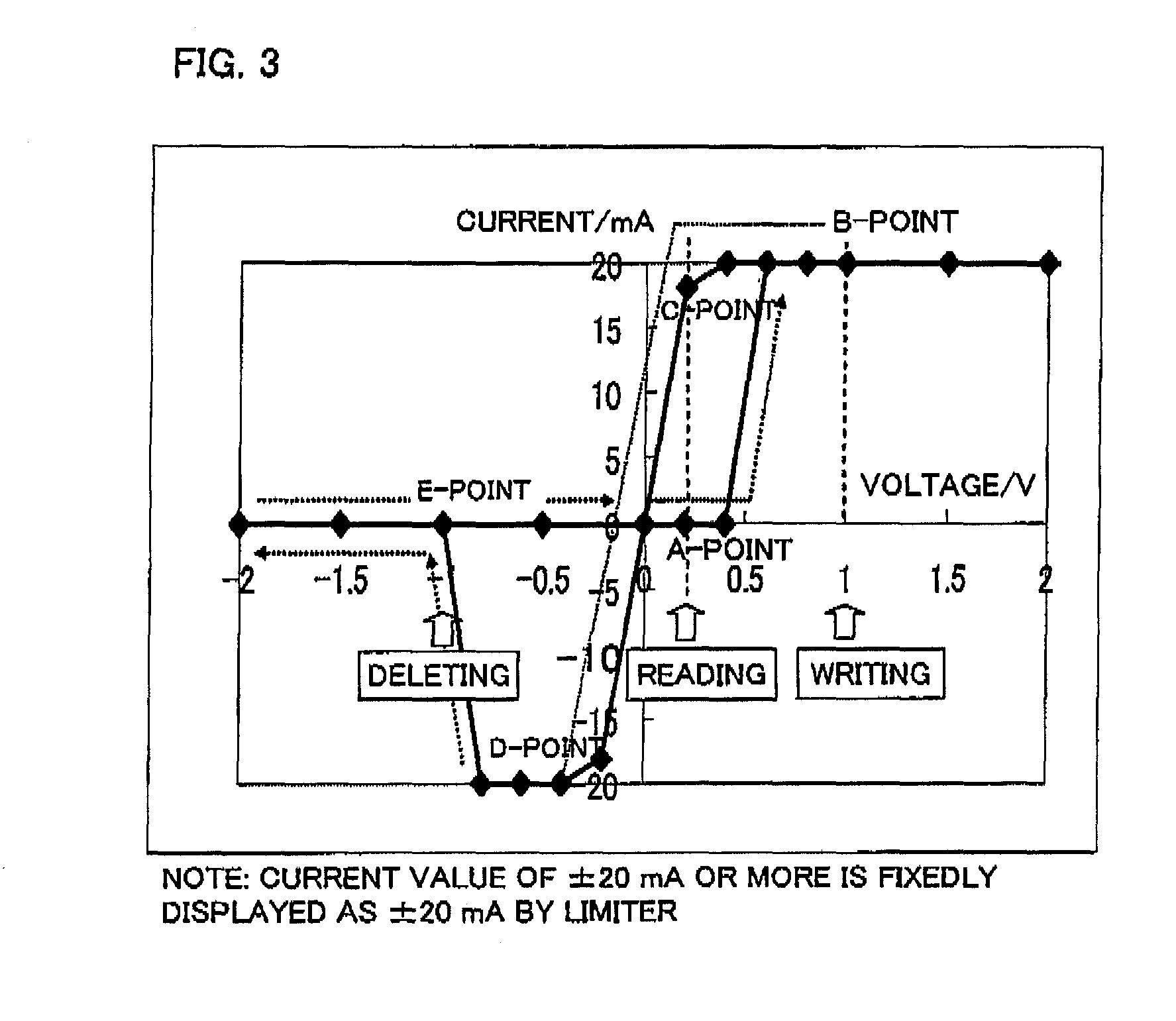
[0104]A resistance value measuring circuit shown in FIG. 6 was used. A change in resistance value of the memory element obtained in Example 1 was measured using a high-speed oscilloscope. FIG. 7 shows data indicating the change in resistance value. As is apparent from FIG. 7, a time for shift from a high resistance (22 MΩ) to a low resistance (2Ω) when a voltage of 1 V was applied between electrodes was 0.02 μs (20 ns). Thus, it is apparent that a write time is equal to or smaller than 50 ns even when a time lag is taken into account.

[0105]FIG. 8 shows an example of a 4×4-memory fundamental circuit using the nonvolatile memory according to the present invention.

[0106]Each memory...


PUM


Abstract

To provide a nonvolatile memory which realizes nonvolatile characteristic similar to a flash memory and a high-speed access equivalent to SRAM, has an integration degree exceeding that of DRAM, requires low voltage and low power consumption, and can be driven by a small-size battery, there are provided: (1) a non-volatile memory, including: a pair of metal electrodes; and a nano-hole-containing metal oxide film having a film thickness of 0.05 μm to 5 μm, which has a honeycomb structure and is provided between the pair of metal electrodes in a Schottky junction state, to use an interface state produced in a partition wall of the nano-hole-containing metal oxide film as a memory charge holder; and (2) a non-volatile memory, including: a substrate electrode; a nano-hole-containing metal oxide film formed by anodic oxidation of a surface of the substrate electrode; and a metal electrode formed to an upper end portion of a partition wall of the nano-hole-containing metal oxide film by Schottky junction, in which the nano-hole-containing metal oxide film has a structure in which a plurality of double Schottky barriers are formed in parallel.

Description

TECHNICAL FIELD[0001]The present invention relates to a non-silicon nonvolatile memory. More particularly, the present invention relates to a nonvolatile memory using interface states produced in partition walls of a nano-hole-containing metal oxide film as memory charge holders.BACKGROUND ART[0002]There have been used general-purpose random access memories that are a static RAM (SRAM: random access read / write memory which requires no memory holding (refresh) operation), a dynamic RAM (DRAM: random access read / write memory which requires refresh operation), and a flash memory (nonvolatile semiconductor memory having both a feature of a RAM and a feature of a ROM capable of holding data after the power-off).[0003]In addition to the defect that the SRAM is volatile, a capacity thereof cannot be increased because it is difficult to realize high integration thereof. However, high-speed access is possible, so the $RAM is used for a cash memory and the like. In addition to the defect that...

Claims


Application Information

Patent Timeline
Patent Type & Authority Applications(United States)
IPC IPC(8): H01L29/47
CPCG11C13/0007G11C2213/15G11C2213/32H01L29/872H01L27/1021H01L29/8616G11C2213/34
Inventor NIGO, SEISUKEOHNISHI, TAKAYUKI
Owner MISUZU R&D
Why Eureka
Try Eureka