Optical Semiconductor Device

a semiconductor and optical technology, applied in the field of optical semiconductor devices, can solve the problems of inability to apply light laterally, inability to achieve alignment-free, and inability to improve coupling efficiency and maintain stability, and achieve the effects of improving and stabilizing coupling efficiency, simple structure, and small siz

Inactive Publication Date: 2008-09-11
CANON KK
View PDF36 Cites 26 Cited by
  • Summary
  • Abstract
  • Description
  • Claims
  • Application Information

AI Technical Summary

Benefits of technology

[0011]According to an optical semiconductor device of the present invention, a photoconductive element can be provided in which a gap spacing between electrodes and an electric field across the gap can be controlled with a simple structure. In addition, a structure can be provided which improves and stabilizes coupling efficiency in coupling with light to be applied to the gap portion. In view of the foregoing, there can be provided a terahertz sensing device capable of operating at a low voltage, in a small size, with a sensing optical system being easily adjustable, and with high stability and S / N ratio. Using this sensing device, it is possible to perform analysis of a biological material, an organic substance, or a semiconductor material, noninvasive and noncontact sensing of human body, sensing of a positional change of an object, and the like, at a low cost with high sensitivity.

Problems solved by technology

In the integrated device discussed above, it is difficult to improve coupling efficiency and to maintain stability because a laser beam is aligned with a photoconductive element by spatial coupling.
Since the gap portion of the photoconductive element is formed on the substrate surface, it is impossible to apply light laterally.
Thus alignment-free cannot be achieved by providing an optical waveguide on a substrate.
In other words, there remain problems to be solved such as sensitivity in sensing, a total measurement time, and manufacturing costs.
Furthermore, since an electric field is applied through a surface electrode, an internal electric field of LT-GaAs is not uniform and the behavior of a carrier excited by a laser beam cannot be controlled efficiently.
In addition, in terms of gap spacing, accurate photolithography is required to form a narrow gap of 1 μm or less with high reproductivity for controlling electric field intensity, thereby leading to an increase in manufacturing cost.
Not only an integrated device but also a single photoconductive element allowing an electromagnetic wave to propagate through space has a similar problem.

Method used


Image

  • Optical Semiconductor Device
  • Optical Semiconductor Device
  • Optical Semiconductor Device

Examples


first embodiment

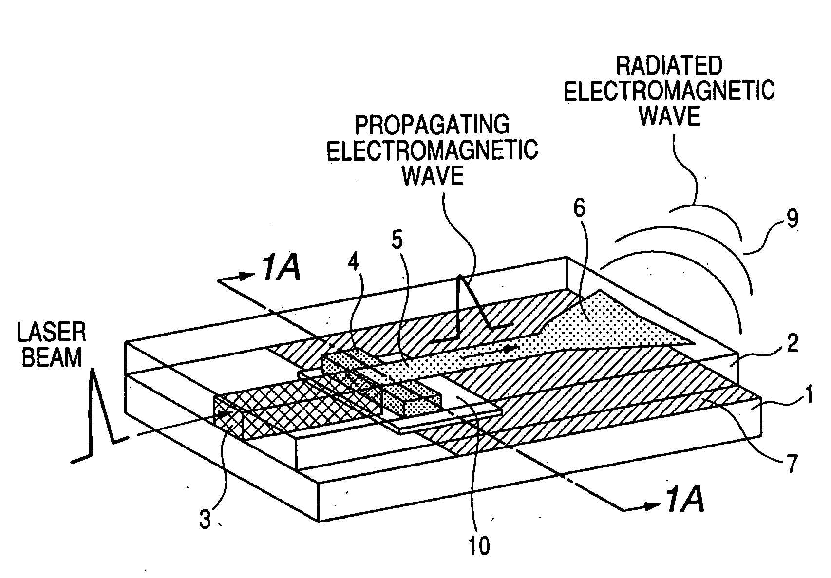
[0029]According to a first embodiment of the present invention, an optical waveguide, a microstrip line, and a photoconductive element for converting light into a terahertz electromagnetic wave are integrated on the same substrate, as shown in FIG. 1.

[0030]A Ti / Au electrode (or an Al electrode) 7 serving as a ground plane is formed in a partial region on an Si substrate 1. A low-temperature (LT)-grown GaAs epitaxial film 4 having a thickness of 2 μm is transferred in the vicinity of the center. An optical waveguide 3 is formed on the left side of the LT-GaAs such that an externally-incoming beam efficiently performs photoirradiation to the side surface of the LT-GaAs film. On the other hand, a microstrip line 5 of Ti / Au is formed on the right side on the top with an insulator 2 interposed such that an electromagnetic wave generated at LT-GaAs can propagate. This line also serves as an upper electrode of LT-GaAs. A patch antenna 6′ is formed on the other end portion of the line such ...

second embodiment

[0048]According to a second embodiment of the present invention, a plurality of elements are arrayed on the same semiconductor substrate as shown by an integrated device 40 in FIG. 4. In the manufacturing process shown in the first embodiment, the elements are formed on an Si substrate 41 collectively on a wafer level, so that arrayed elements can be provided freely depending on the arrangement of the element or how the wafer is cut.

[0049]More specifically, two optical waveguides 42a and 42b, photoconductive elements 47a and 47b, microstrip lines 43a and 43b, and print dipole antennas 44a and 44b are arrayed in parallel. Although the array spacing is illustrated as 1 cm herein, the present invention is not limited thereto. In this case, a THz electromagnetic wave includes a component propagating through space as shown by an arrow 46, so that the changing state of the electromagnetic wave reflected on an object 45 can be detected.

[0050]In terms of an optical system, while a femto-sec...

third embodiment

[0054]According to a third embodiment of the present invention, as shown in FIG. 5, two photoconductive elements are integrated on the same substrate. This allows a sensor device to function on one substrate for sensing an object placed closely on a high frequency transmission line.

[0055]A photoconductive element 53a is similar to that in the first embodiment in that, with application of a vertical electric field between a line 54 and a lower electrode 52a, a THz electromagnetic wave, which is excited by light propagating through an optical waveguide 51a, propagates through the line 54. In this embodiment, a ground plane is not provided, and a high frequency transmission line is a single line including the signal line 54 embedded in an insulator 55 upward and downward. Electrodes 52a and 52b are isolated, each having a thickness of about 3 μm with Au plating for adjusting the height of the photoconductive element.

[0056]Therefore, the manufacturing process is almost the same as in th...


PUM


Abstract

The present invention provides an optical semiconductor device including a semiconductor thin film (4) having photoconductivity and a pair of electrodes (5) and (10) for applying an electric field to an inside of the semiconductor thin film (4) in a direction approximately vertical to a surface of the semiconductor thin film (4), wherein the semiconductor thin film (4) generates an electromagnetic wave when light is applied to a region thereof to which the electric field is applied. The electrodes are provided to a front surface and a back surface of the semiconductor thin film (4) with the semiconductor thin film interposed therebetween.

Description

TECHNICAL FIELD[0001]The present invention relates to an optical semiconductor device functioning as a device for generating and detecting a high frequency electromagnetic wave mainly in a region from a millimeter wave to a terahertz wave using light irradiation.BACKGROUND ART[0002]In recent years, there has been developed a nondestructive sensing technique using an electromagnetic wave (30 GHz to 30 THz) ranging from a millimeter wave to a terahertz (THz) wave. Techniques under development in the application field of the electromagnetic wave having this frequency band include a technique for carrying out imaging using a safe radioscopic inspection system in place of an X-ray system, a spectroscopic technique for obtaining an absorption spectrum or a complex dielectric constant of the inside of a substance to evaluate a coupling state of atoms, a technique for analyzing a biomolecular, and a technique for evaluating concentration or mobility of carriers.[0003]JP10-104171A discloses ...

Claims


Application Information

Patent Timeline
Patent Type & Authority Applications(United States)
IPC IPC(8): G01J5/00H01L31/18H01L31/09
CPCG01N21/3581H01S1/02H01L31/08
Inventor OUCHI, TOSHIHIKOITSUJI, TAKEAKIKASAI, SHINTARO
Owner CANON KK
Why Eureka
Try Eureka