Composition for polishing semiconductor wafer, and method of producing the same

a technology of semiconductor wafers and polishing methods, which is applied in the direction of manufacturing tools, lapping machines, other chemical processes, etc., can solve the problems of affecting the yield and quality of semiconductor products, scratching easily on the polished surface, and contaminating a surface subjected to high-precision processing, etc., to achieve excellent polishing ability

Inactive Publication Date: 2008-10-02
NIPPON CHECMICAL IND CO LTD +1
View PDF9 Cites 34 Cited by
  • Summary
  • Abstract
  • Description
  • Claims
  • Application Information

AI Technical Summary

Benefits of technology

[0032]The use of the polishing composition according to the present invention can provide significant advantages in polishing of a semiconductor wafer or the like. According to the present invention, a polishing composition which has an excellent polishing ability lasting for a long time in the mirror polishing of a wafer, which has been unsatisfactory to date, can be provided. Accordingly, the present invention provides a significant advantage to the related industrial field.

Problems solved by technology

If the outer circumferential edge of the wafer has an irregular shape during transferring, the following problems may occur.
Furthermore, contaminating particles may intrude into such a rough surface and be scattered in the subsequent steps, thereby contaminating a surface that has been subjected to high-precision processing.
These problems significantly affect the yield and the quality of the semiconductor products.
However, in this case, scratches are easily formed on the polished surface.
However, the dispersion containing silica having an average secondary particle diameter of 30 nm described in Claim 1 of document '004 cannot be produced by the grinding method using a high-pressure homogenizer.
When a high-pressure homogenizer is used for fine grinding under a severe condition, a diamond member provided at an impact portion is worn out, thus producing a contamination component of the silica dispersion.
Furthermore, replacing the diamond member requires a high cost.
Therefore, this method is not employed as an industrial grinding method.
Accordingly, the particle diameters of these silica particles are too small to be suitable for use in a polishing agent.
Furthermore, according to paragraph 0022 of the specification, the use of a bead grinding method decreases the grinding efficiency and the production efficiency because of, for example, formation of ultrafine particles and polydispersity.
However, commercially available fumed silica is used without further treatment in the techniques described in each of these patent documents.
Accordingly, disadvantages of fumed silica have not been fundamentally solved.
Accordingly, even if a known composition for polishing a surface of a semiconductor wafer is used under such process conditions, a satisfactory polishing speed and a satisfactory surface roughness cannot be obtained.

Method used


Image

  • Composition for polishing semiconductor wafer, and method of producing the same
  • Composition for polishing semiconductor wafer, and method of producing the same
  • Composition for polishing semiconductor wafer, and method of producing the same

Examples


examples 3 to 7

[0095]Preparation of Slurry C: Slurry A1 was Mixed with commercially available colloidal silica particles (Silicadol, silica concentration: 40 weight percent, manufactured by Nippon Chemical Industrial Co., Ltd.) having a particle diameter of 50 nm and purified water at mixing ratios shown in Table 1, thus allowing Slurry C1 to Slurry C5 (Examples 3 to 7) to be prepared.

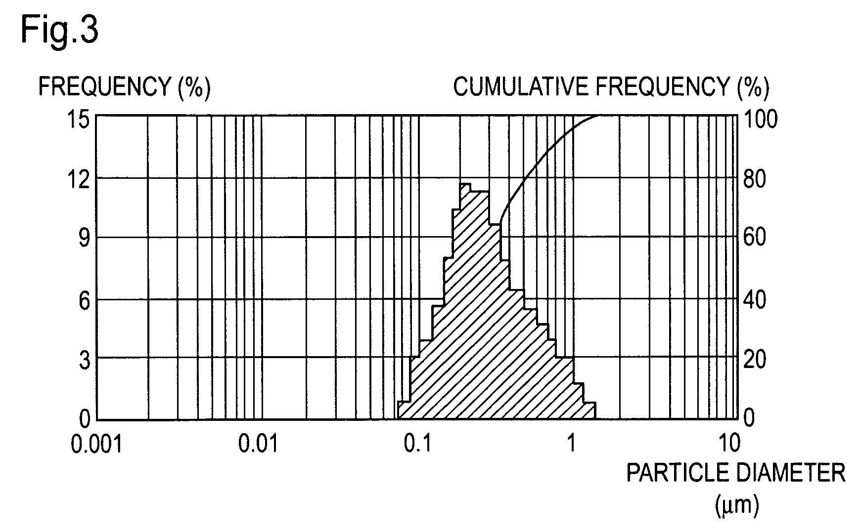
[0096]Table 2 summarizes physical properties of each of the slurries prepared as described above.

TABLE 1ColloidalPurifiedA1sillicawaterSilicaParts byParts byParts byconcentrationSlurry Cweightweightweightwt %C111.250.7525C211.500.9025C312.001.2025C413.001.8025C515.003.0025

TABLE 2AverageSilicaBET specificparticleconcentrationsurface areadiameterSlurrywt %pHm2 / gA / BnmA02510.23955266A1259.061291.523.2B0209.65143535.3B1209.041701.538.7C12510.1C22510.0C3259.9C4259.8C5259.8

[0097]Each of the silica slurries was diluted with purified water to a predetermined silica concentration. Chemicals shown in Tables 3 and 4 were then ad...

example 33

A Grinding Example in which a Slurry is Passed Through a Bead Mill Twice Using Beads Having a Diameter of 0.1 mm

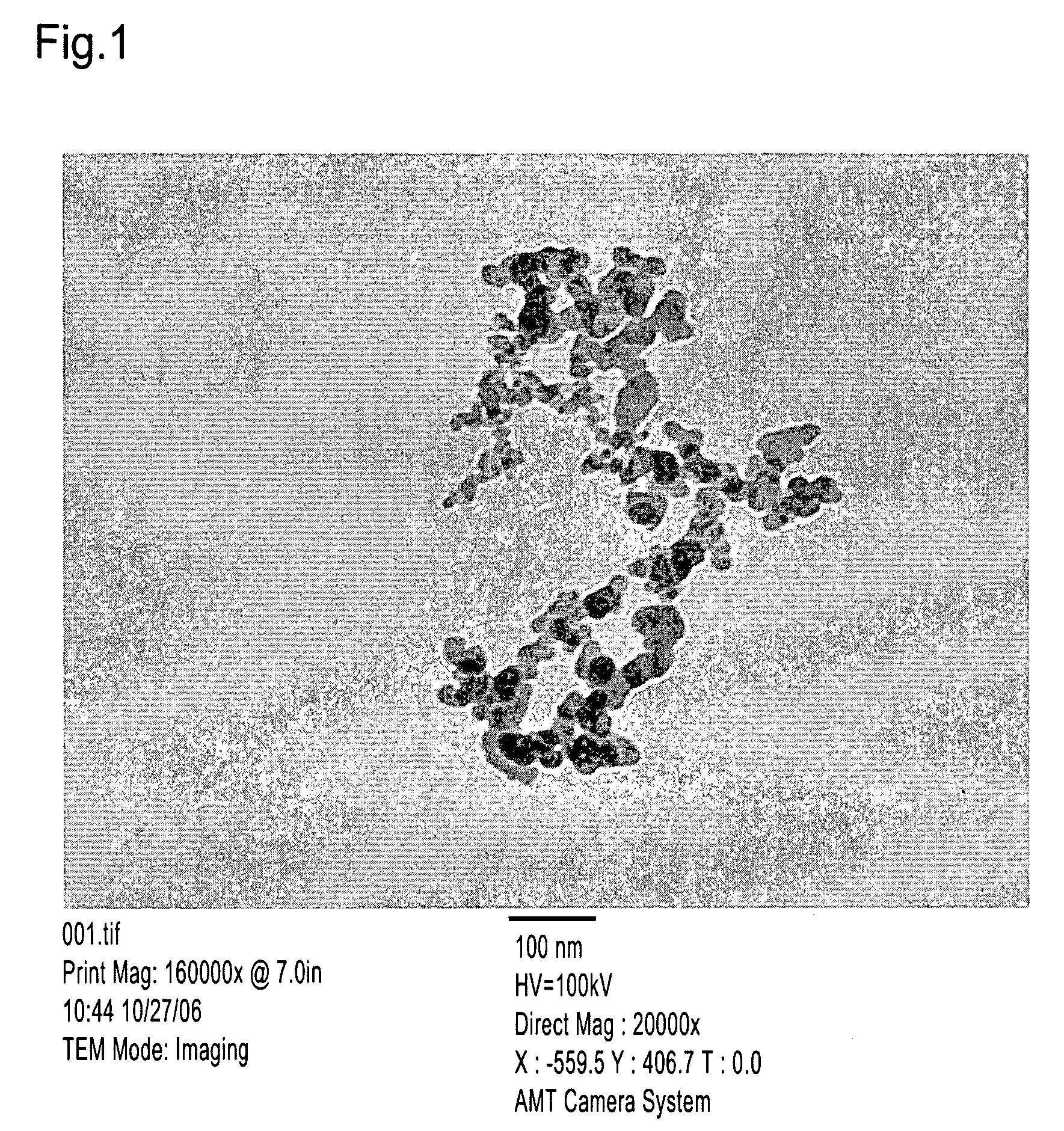
[0124]Tetramethylammonium hydroxide was added to 75 parts by weight of purified water in an amount of 0.15 mol relative to 1 kg of silica, and mixing was performed under stirring. Subsequently, 25 parts by weight of the same fumed silica particles as those used in Slurry A of the above examples (BET specific surface area: 90 m2 / g) were added to the mixture and dispersed by agitation. Thus, a slurry containing 25 weight percent of silica was prepared. The pH of this slurry was 10.23, and the BET specific surface area of the silica particles in the slurry was 95 m2 / g. The average ratio A / B of the major axis A to the minor axis B of the silica particles measured by TEM observation was 5. The average particle diameter measured by the laser light-scattering method was 266 nm.

[0125]Subsequently, this slurry was ground with a bead mill (LMZ 2: manufactured by Ashizawa Finetech Lt...

example 34

A Grinding Example Using Beads Having a Diameter of 0.2 mm

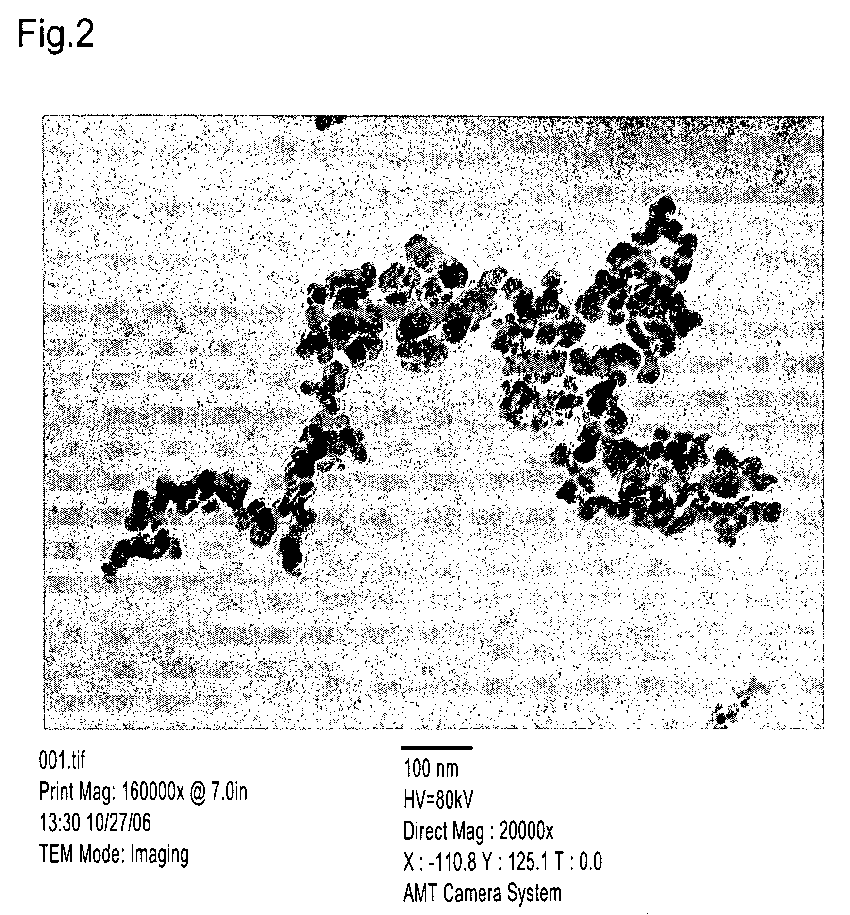
[0126]Tetramethylammonium hydroxide was added to 75 parts by weight of purified water in an amount of 0.15 mol relative to 1 kg of silica, and mixing was performed under stirring. Subsequently, 25 parts by weight of commercially available fumed silica particles (BET specific surface area: 90 m2 / g) were added to the mixture and dispersed by agitation. Thus, a slurry containing 25 weight percent of silica was prepared. The pH of this slurry was 10.23, and the BET specific surface area of the silica particles in the slurry was 95 m2 / g. The average ratio A / B of the major axis A to the minor axis B of the silica particles measured by TEM observation was 5. The average particle diameter measured by the laser light-scattering method was 266 nm.

[0127]Subsequently, this slurry was ground with a bead mill (LMZ 2: manufactured by Ashizawa Finetech Ltd.) using zirconia beads having a diameter of 0.5 mm as a grinding medium at a slurry fl...


PUM

PropertyMeasurementUnit
specific surface areaaaaaaaaaaa
particle diameteraaaaaaaaaa
diameteraaaaaaaaaa

Abstract

A composition for polishing a semiconductor wafer contains fumed silica particles that are produced by wet grinding using a grinding medium and that have characteristics (A) to (C):
(A) a specific surface area in the range of 50 to 200 m2/g measured by a BET method;
(B) an average particle diameter in the range of 10 to 50 nm measured by a laser light-scattering method; and
(C) an average ratio A/B of the major axis A to the minor axis B of the fumed silica particles in the range of 1.2 to 2.0 measured by TEM observation,
wherein the concentration of silica particles containing the fumed silica particles is in the range of 0.5 to 50 weight percent relative to the total weight of an aqueous dispersion.

Description

BACKGROUND OF THE INVENTION[0001]1. Field of the Invention[0002]The present invention relates to a composition for wafer polishing in which polishing is performed on a surface and an edge portion of a semiconductor wafer such as a silicon wafer or a semiconductor device substrate having a metal film, an oxide film, a nitride film, and the like (hereinafter referred to as “a metal film and the like”) thereon, and a method of producing the same. Furthermore, the present invention relates to a processing method of forming a mirror surface of a surface or an edge portion of a semiconductor wafer using the composition for wafer polishing.[0003]2. Description of the Related Art[0004]Electronic components such as ICs, LSIs, and VLSIs, which are made of a semiconductor material, e.g., silicon single crystal, as a raw material, are produced from a small piece of semiconductor element chip prepared by forming a large number of fine electrical circuits on a wafer, which is prepared by slicing ...

Claims


Application Information

Patent Timeline
Patent Type & Authority Applications(United States)
IPC IPC(8): C09K13/02C09K3/14B24B37/00B82Y10/00B82Y99/00H01L21/304
CPCC09G1/02H01L21/02024
Inventor MAEJIMA, KUNIAKINAKAJO, MASARUTANAKA, HIROAKI
Owner NIPPON CHECMICAL IND CO LTD
Why Eureka
Try Eureka