[0007]The object of the present invention is to provide an energy efficient, fine gray scale, full-color, high-brightness, high-definition, large-screen, long-lived, moving-picture
projection display system in multiple formats that can be manufactured at low cost. This objective is achieved by provision, in the projection display
system, transmission-mode optically addressed, spatial light modulators (OASLMs) that can modulate read light beams substantially spanning the
visible spectrum, can be written with available and inexpensive
ultraviolet write light sources, can switch sufficiently fast to avoid perceptible image
lag and image
ghosting, and require no pixilation, thereby avoiding expense and inter-pixel obscuration. An
advantage of the invention is that it allows the display to change electronically the pixilation format of the image it presents, e.g., from
NTSC to HDTV, according to the nature of the input
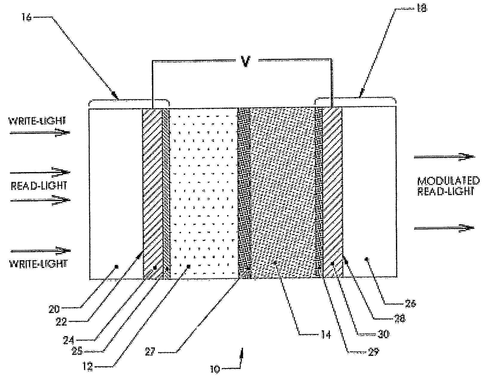
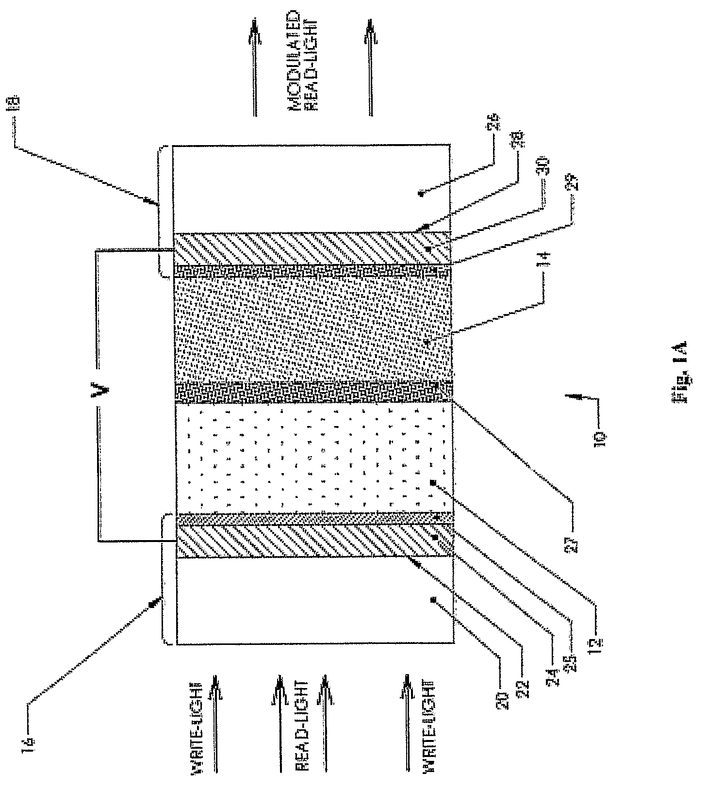
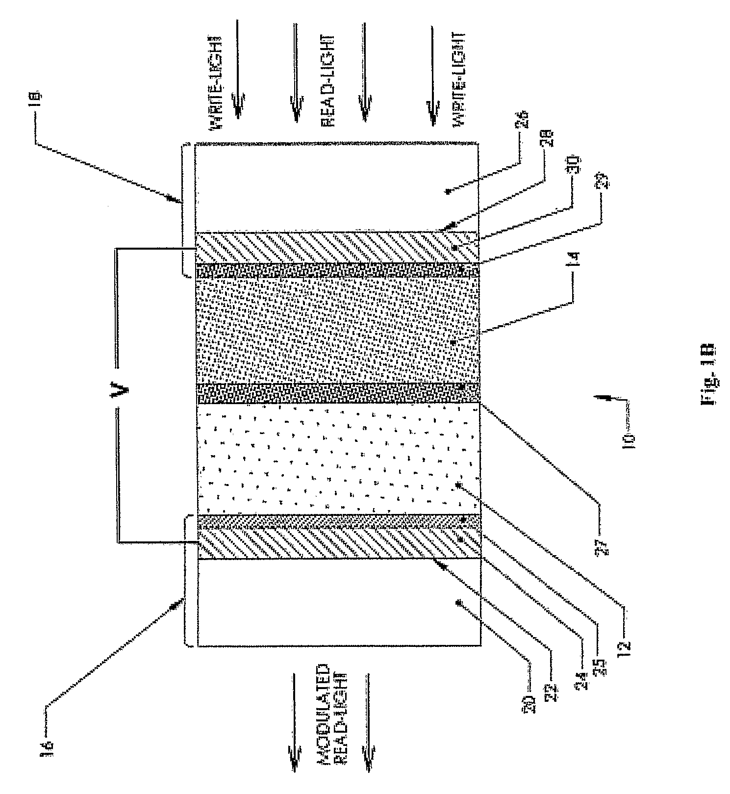
signal, with no exchange or reconfiguration of hardware. The transmission-mode OASLM is implemented with a
light valve structure that does not absorb too much of the various read light beams, uses a nematic
liquid crystal that allows a fine gray scale, is more energy efficient than corresponding OASLMs that use ferroelectric type liquid crystals, and is incorporated in a novel optical engine.
[0008]Preferred embodiments of the invention implement a light projection display system using one or more optically addressed
spatial light modulator (OASLM) read valves that operate in a transmissive mode and are individually or collectively capable of modulating a wide spectrum of visible read light, as well as sources of the read light and the optical engine. Some of the preferred embodiments of the invention use one or more electrically addressed write valve SLMs of the type known as
liquid crystal on
silicon (LCOS) as well as sources of the write light. Other preferred embodiments use electrically addressed write valve SLMs of the types known as
amorphous silicon or
polycrystalline silicon thin-film
transistor (TFT) displays as well as sources of the write light. Another preferred embodiment uses a digital mirror as the write
light valve as well as sources of the write light. Still other of the preferred embodiments use devices chosen from the group of
cathode ray tubes (
CRTs),
field effect display (FED) devices, inorganic
light emitting diode (LED) arrays, organic
light emitting diode (
OLED) arrays, and
plasma displays that both provide the write light and impose the modulation of its intensity required to write the proper pattern into the read valve OASLMs together with a simpler optical engine.
[0009]Each read valve OASLM absorbs most of the write light, which is used to define the portion of the image that is rendered in the corresponding color of read light, within a photoconductive structure. Each read valve OASLM passes most of the read light (visible illumination light) through the same photoconductive structure that absorbs the corresponding write light. (Some absorption and reflection is unavoidable but undesired.) Each read valve OASLM also passes most of its read light through a nematic
liquid crystal structure, in which the polarization state of the read light is modulated by the local state of the liquid
crystal according to the local value of the
electric field across the liquid
crystal. The series combination of the photoconductor structure and the nematic liquid
crystal structure forms a sandwich that is positioned between
electrode structures on either side of the sandwich. The local value of the
electric field is determined by the total
electric field applied by the
electrode structures across the sandwich and by the local value of the fraction of this total
voltage that falls across the photoconductive structure, which is affected by the local amount of the
photocurrent of electrons and holes that the write light has excited in each local region. There is no pixel structure or native pixel resolution in any of the read valve OASLMs. Thus, changing the pixilation format entails changing the pixilation format of the write light pattern going into the read valve OASLMs.
[0010]Because the photoconductive structure absorbs most of the write light and transmits most of the read light, the bands of wavelengths of light used for the two beams for each read valve OASLM are substantially non-overlapping. In preferred embodiments, wavelengths in the band of wavelengths of write light are shorter than those in the band of wavelengths of the corresponding read light in each read valve OASLM. The read light must not erase the pattern written by the write light, even though the
photon flux (i.e., integrated power) of the read light is predominant over that of the write light. For preferred embodiments that use violet read light, the corresponding write light is in the
ultraviolet (UV) range of the
electromagnetic spectrum. Thus, read valve OASLMs for blue and violet read light require photoconductive materials that transmit
blue light but absorb UV light to produce sufficient
photoconductivity. The photoconductive materials of the prior art do not meet this requirement for blue read valves operating in a transmissive mode. Although it mentioned the possibility of a transmissive mode
full color display and suggested that an OASLM might use ZnS as the photoconductive material, U.S. Pat. No. 3,824,002, neither taught nor provided a drawing figure of such a device. Moreover, there is no available supply of ZnS that is sufficiently transparent for
blue light to make a practical
full color projection
display device. Specifically, the
photocurrent across the photoconductive structure of the OASLM produced by a unit of blue
light energy at a
wavelength of about 420 nm would be approximately 1,000 times less than the corresponding
photocurrent produced by unit of
ultraviolet light energy at a practical
wavelength of about 370 nm.
[0011]It is well known that liquid crystal cells degrade over time if they are subjected to long-time sustained DC electrical bias of greater than about 0.1 V. Therefore, display devices using liquid crystal cells in OASLMs and intended for long service lives should not be implemented with OASLM structures that rectify to any substantial degree the AC
voltage signals applied to them. For the same reason, the photoconductive structures with the OASLMs should not be implemented to act as photodiodes.
[0012]For those embodiments in which the source of write light is separate from the write
light valve that imposes the pattern in its intensity, the write light propagates from a write
light source to a write valve SLM that modulates it according to electronic signals coming from an
electronic data system to begin the image definition process of the display. The modulated write light from each write valve propagates further to a read valve SLM, where it controls the modulation of the corresponding beam of read light, as just described above. In various preferred embodiments, the write valve SLM is chosen from the group of possible components that includes an
electrode array type SLM, such as a liquid crystal-on-
silicon (LCOS) or a
thin film transistor (TFT) array device; a digital mirror array; and an OASLM written by an electro-optically steered, focused beam of light of a band of
wavelength and operating in either the reflection mode or the transmission mode. If operating in the transmission mode, the light that writes this write valve substantially non-overlaps the band of write light for that OASLM and is absorbed in the photoconductor of that OASLM while the write light that is modulated therein is not substantially absorbed in the photoconductor. After passing through the read valve SLM, the intensity of the visible read light is modulated by a
linear polarization filter (or other technique known in the art) in accordance with the two-dimensional pattern that was imposed by the write light and is then projected as an image onto a display screen, either from the front or from the rear.


