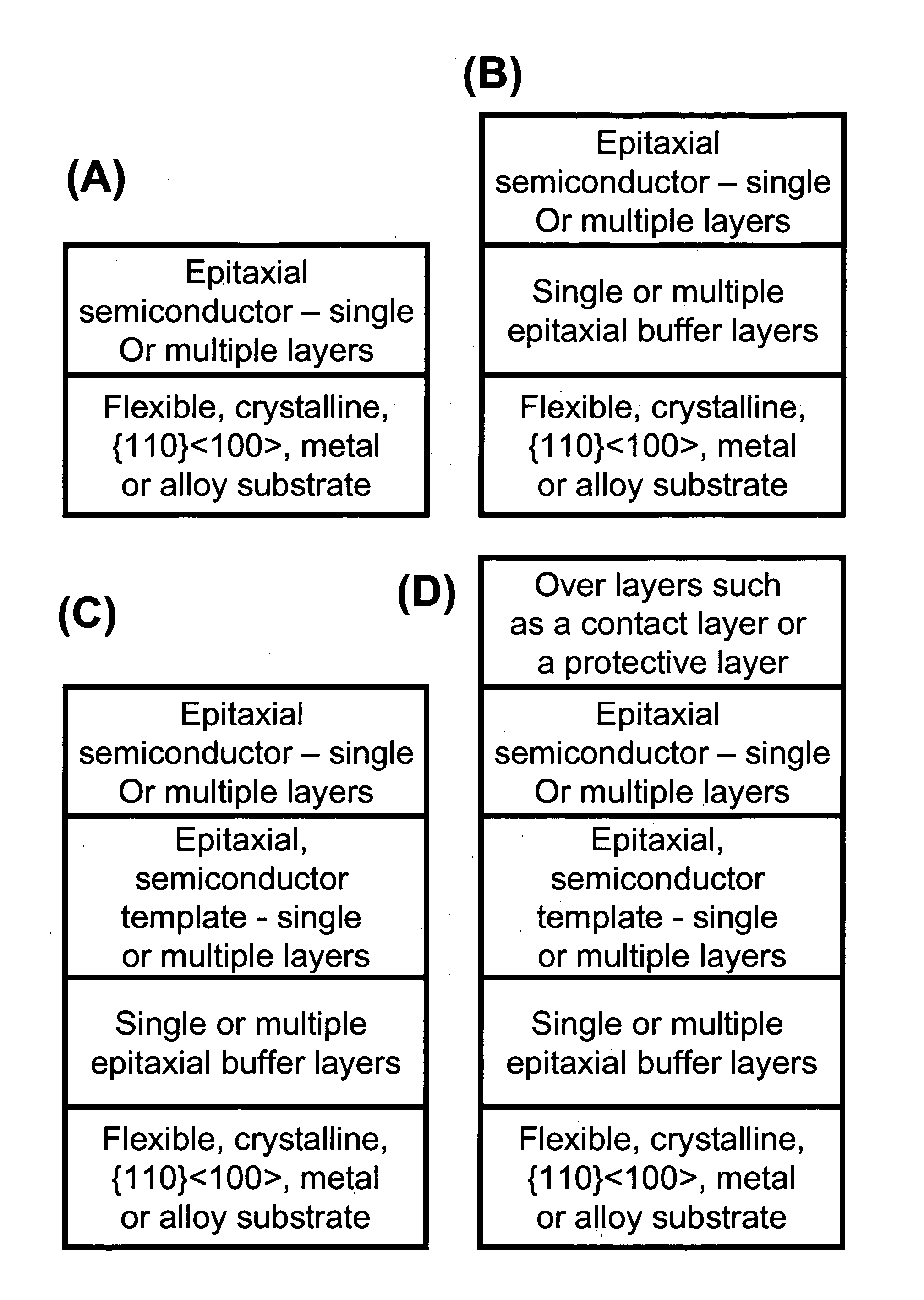
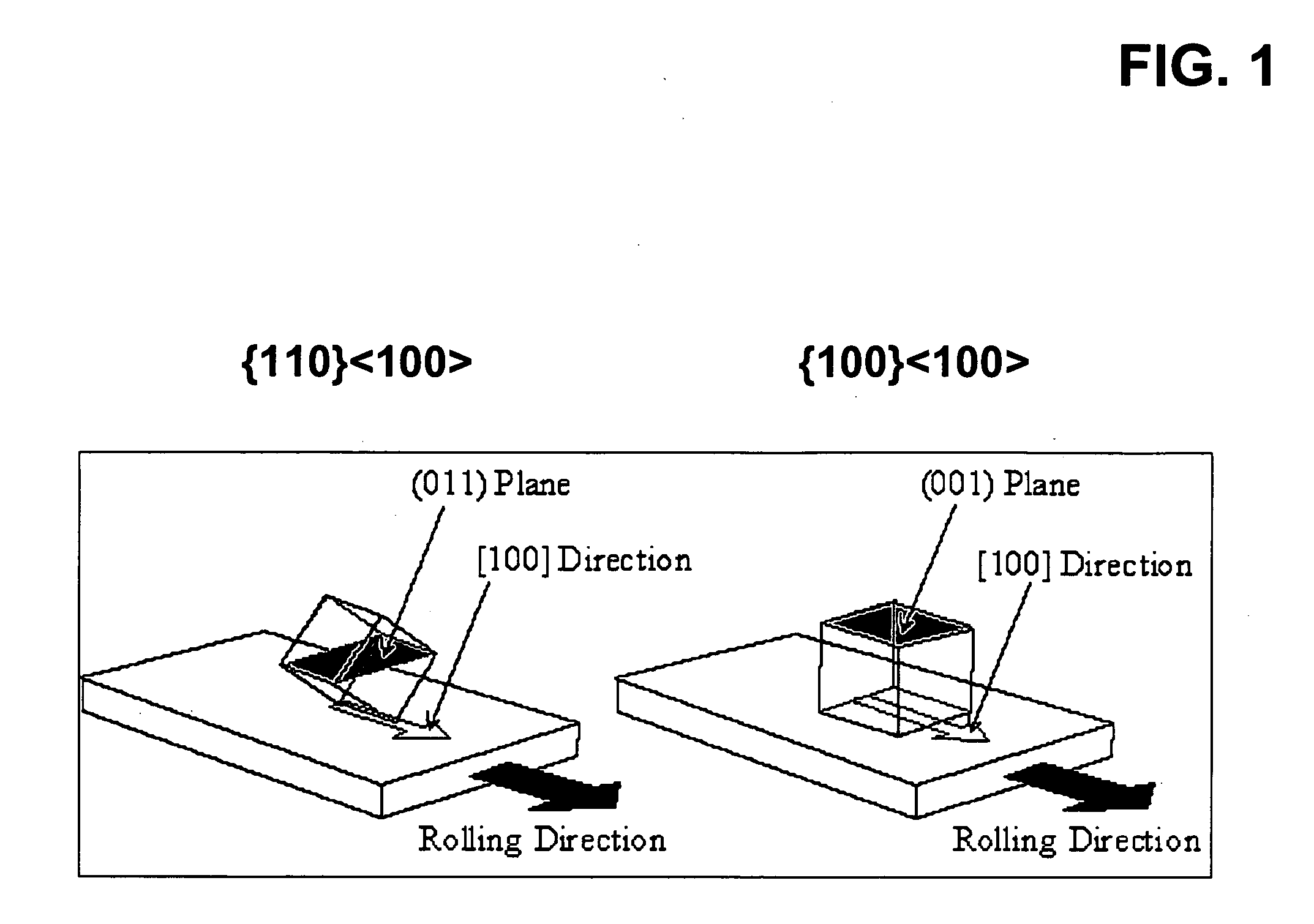
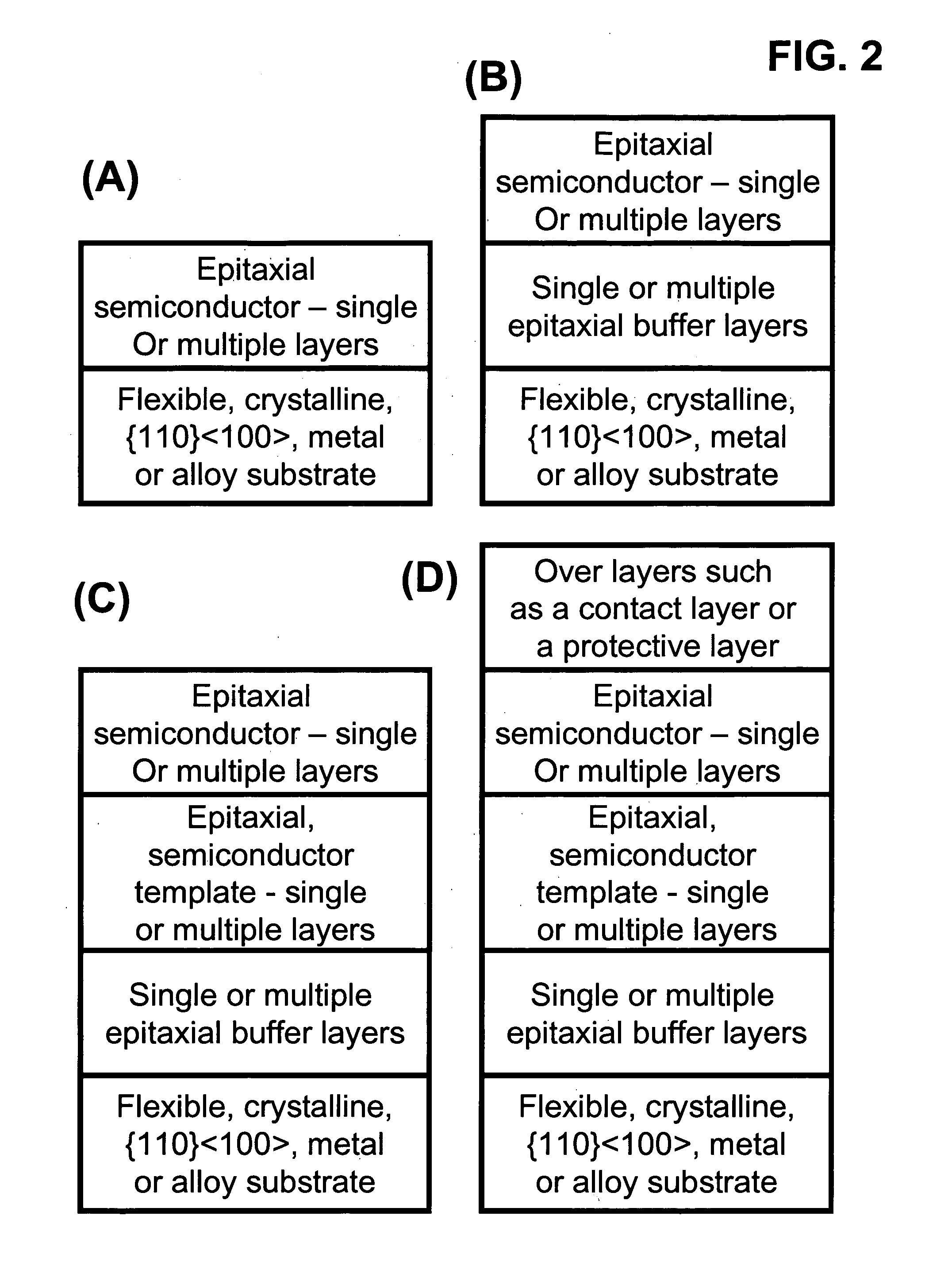
Semiconductor-based, large-area, flexible, electronic devices on <100> oriented substrates

a technology of semiconductors and substrates, applied in the field of semiconductor-based, large-area, flexible, electronic devices on <100> oriented substrates, can solve the problems of unrealized solar energy promise, prohibitively expensive cost of single crystal substrates, unfavorable price/performance metric, etc., and achieve high performance

Inactive Publication Date: 2008-10-30
GOYAL AMIT
View PDF12 Cites 52 Cited by
  • Summary
  • Abstract
  • Description
  • Claims
  • Application Information

AI Technical Summary

Benefits of technology

[0011]The invention relates to fabrication of large-area, flexible, semiconductor based electronic devices whic

Problems solved by technology

However, for the past two decades, the promise of solar energy has remained unrealized.
This is primarily because of the unfavorable price/performance metric of solar cells being manufactured today.
While a complete understanding of the microstructural features which limit the performance are still unclear, it is reasonably well established that recombination at grain boundaries, intragrain defects and impurities is critical.
Most thin-film solar cells are based on polycrystalline device layers since the cost of single crystal substrates

Method used


Image

  • Semiconductor-based, large-area, flexible, electronic devices on &#x3c;100&gt; oriented substrates
  • Semiconductor-based, large-area, flexible, electronic devices on &#x3c;100&gt; oriented substrates
  • Semiconductor-based, large-area, flexible, electronic devices on &#x3c;100&gt; oriented substrates

Examples


example 1

[0108]Starting with a secondary recrystallized, Fe-3 at % Si substrate, with a {110} orientation, a 10-75 nm thick, epitaxial layer of TiN is grown by electron beam evaporation, sputtering, pulsed laser ablation or chemical vapor deposition at a substrate temperature in the range of 300-850° C. This is followed by deposition of an epitaxial Si layer using chemical vapor deposition in the temperature range of 300-900° C.

example 2

[0109]Starting with a secondary recrystallized, Fe-3 at % Si substrate, with a {110} orientation, a 10-75 nm thick, epitaxial layer of TiN is grown by electron beam evaporation, sputtering, pulsed laser ablation or chemical vapor deposition at a substrate temperature in the range of 300-850° C. This is followed by deposition of a 10-75 nm thick, epitaxial, layer of MgO by electron beam evaporation, sputtering, pulsed laser ablation or chemical vapor deposition at a substrate temperature in the range of 300-850° C. This is followed by deposition of an epitaxial Si layer using chemical vapor deposition in the temperature range of 300-900° C.

example 3

[0110]Starting with a secondary recrystallized, Fe-3 at % Si substrate, with a {110} orientation, a 10-75 nm thick, epitaxial layer of γ-Al2O3 is grown by electron beam evaporation, sputtering, pulsed laser ablation or chemical vapor deposition at a substrate temperature in the range of 300-850° C. This is followed by deposition of an epitaxial Si layer using chemical vapor deposition in the temperature range of 300-900° C. Numerous reports exist in the literature of epitaxial growth of Si on γ-Al2O3 (see for example, Liwen tan, Qiyuan Wang, Jun Wang, Yuanhuan Yu, Zhongli Liu and Lanying Lin, “Fabrication of novel double-hetero-epitaxial SOI structure Si / γ-Al2O3 / Si,” Journal of Crystal Growth, vol. 247, pp. 255-260, 2003; K. Sawada, M. Ishida, T. Nakamura and N. Ohtake, “Metalorganic molecular beam epitaxy of films on Si at low growth temperatures,” Appl. Phys. Lett., vol. 52, pp. 1672-1674, 1988; M. Shahjahan, Y. Koji, K. Sawada and M. Ishida, “Fabrication of resonance tunnel diode...


PUM


Abstract

Novel articles and methods to fabricate the same resulting in flexible, oriented, semiconductor-based, electronic devices on {110}<100> textured substrates are disclosed. Potential applications of resulting articles are in areas of photovoltaic devices, flat-panel displays, thermophotovoltaic devices, ferroelectric devices, light emitting diode devices, computer hard disc drive devices, magnetoresistance based devices, photoluminescence based devices, non-volatile memory devices, dielectric devices, thermoelectric devices and quantum dot laser devices.

Description

CROSS-REFERENCE TO RELATED APPLICATIONS[0001]This application is (1) a continuation-in-part of U.S. patent application Ser. No. 11 / 498,120, which claimed priority to U.S. provisional patent application Ser. No. 60 / 704,264, both of which are herein incorporated by reference in entirety and (2) a continuation-in-part of U.S. patent application Ser. No. 11 / 715,047, filed Mar. 8, 2007, which is also herein incorporated by reference in its entirety.STATEMENT REGARDING FEDERALLY FUNDED RESEARCH OR DEVELOPMENT[0002]This invention was made with Government support under Contract No. DE-AC05-000R22725 awarded by the United States Department of Energy. The Government has certain rights in this invention.FIELD OF THE INVENTION[0003]The invention relates to fabrication of high performance electronic devices comprising various types of semiconductors and articles made therefrom.BACKGROUND OF THE INVENTION[0004]Electronic devices based on semiconductors such as diodes, transistors and integrated c...

Claims


Application Information

Patent Timeline
IPC IPC(8): H01L29/04
CPCB82Y10/00Y02E10/544H01L21/02433H01L21/02439H01L21/02488H01L21/02491H01L21/0251H01L21/02521H01L21/02524H01L21/02538H01L29/78603H01L29/78681H01L29/7869H01L31/036H01L31/0392H01L31/0687H01L31/1872H01L21/02425H01L31/03925H01L31/03928Y02E10/541Y02P70/50
Inventor GOYAL, AMIT
Owner GOYAL AMIT
Why Eureka
Try Eureka