When the P-N junction is reverse biased, however, the junction barrier (and therefore resistance) becomes greater and charge flow is minimal.
Leakage current is a major source of
signal offset and
noise in current photodiode array applications.
Leakage current is temperature dependent; thus, an increase in temperature and
reverse bias results in an increase in leakage or
dark current.
However, at conventional
doping levels utilized for
diode arrays of this type, the
diffusion length of minority carriers generated by
photon interaction in the
semiconductor is in the range of at least many tens of microns, and such minority carriers have the potential to affect signals at diodes away from the region at which the minority carriers were generated.
Thus, an additional
disadvantage with conventional photodiode arrays is the amount and extent of
crosstalk that occurs between adjacent detector structures, primarily as a result of minority
carrier leakage current between diodes.
In almost every area of measurement, the limit to the detectability of signals is set by noise, or unwanted signals that obscure the desired signal.
Noise issues generally have an important effect on device or
system cost.
Conventional photodiodes are particularly sensitive to noise issues.
These noise components collectively contribute to the total noise in the photodiode.
Shot noise tends to dominate when the photodiode is used in photoconductive mode where an external
reverse bias is applied across the device.
As an example, detector noise generated by a planar diffused photodiode operating in the
reverse bias mode is a combination of both
shot noise and thermal noise.
Secondary issues also contribute to dark noise and other noise sources that
impact photodiode sensitivity.
As mentioned above, however, there are numerous problems with conventional photodiodes that attempt to achieve these competing and often conflicting characteristics.
Using a
high resistivity material, however, causes the device to have high dark current.
Since minority
carrier lifetime is limited, many of these photogenerated holes are lost due to recombination of holes and electrons in the bulk material, which causes a reduction in charge collection efficiency or
responsivity of the photodiode.
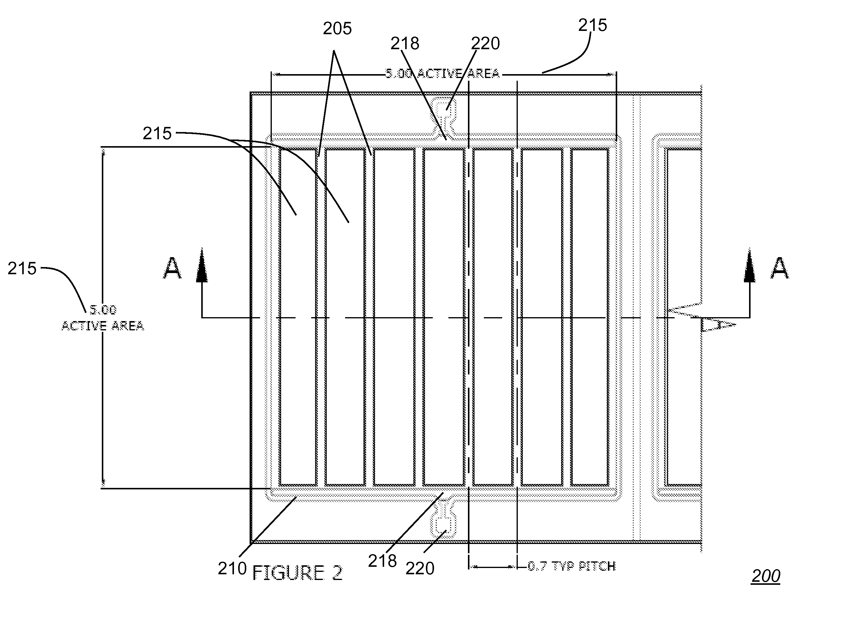
This is disadvantageous, however, because a relatively large number of p+ fishbones is needed when placing the p+ diffused bones closer together, resulting in high junction
capacitance.
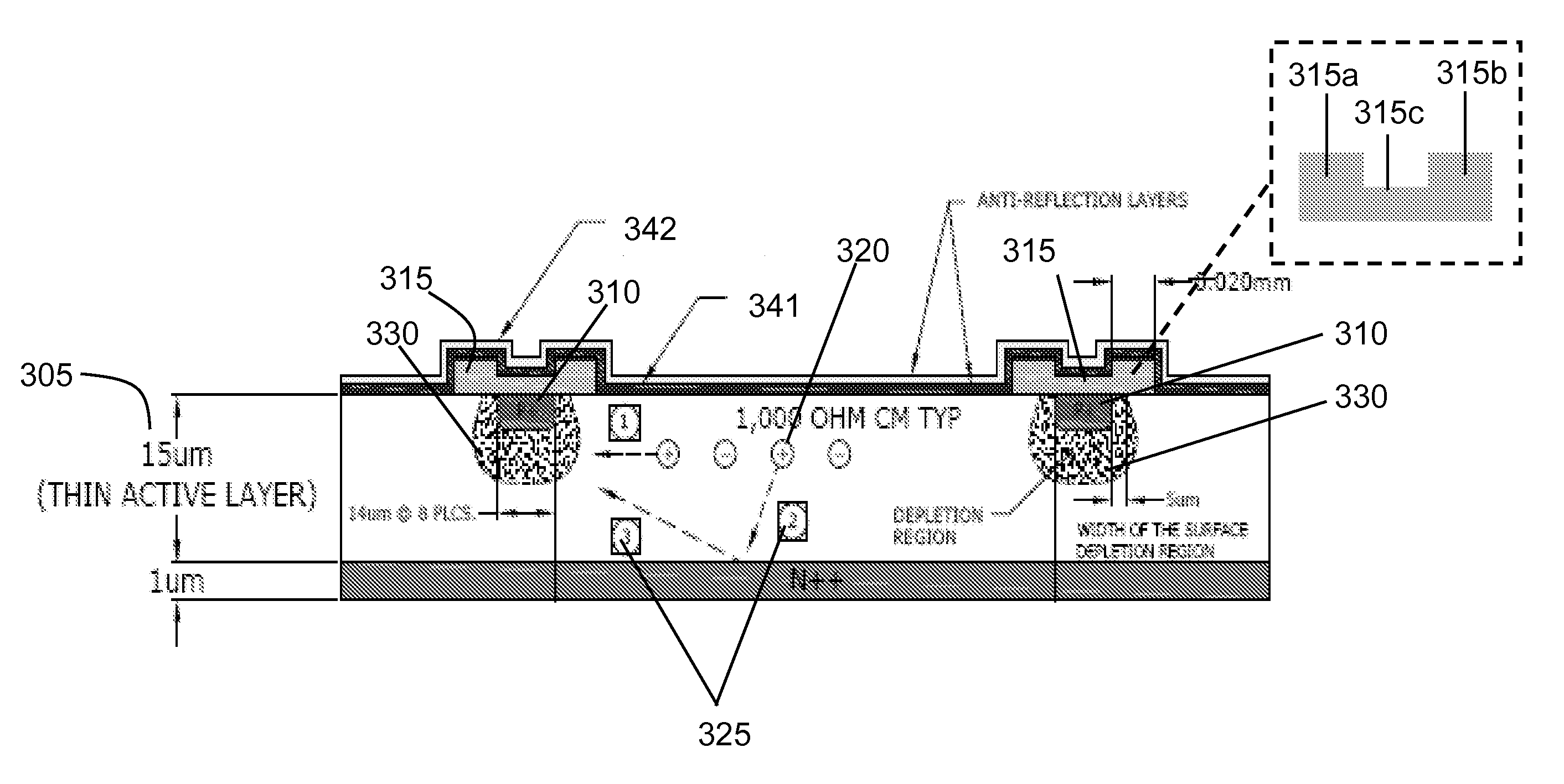
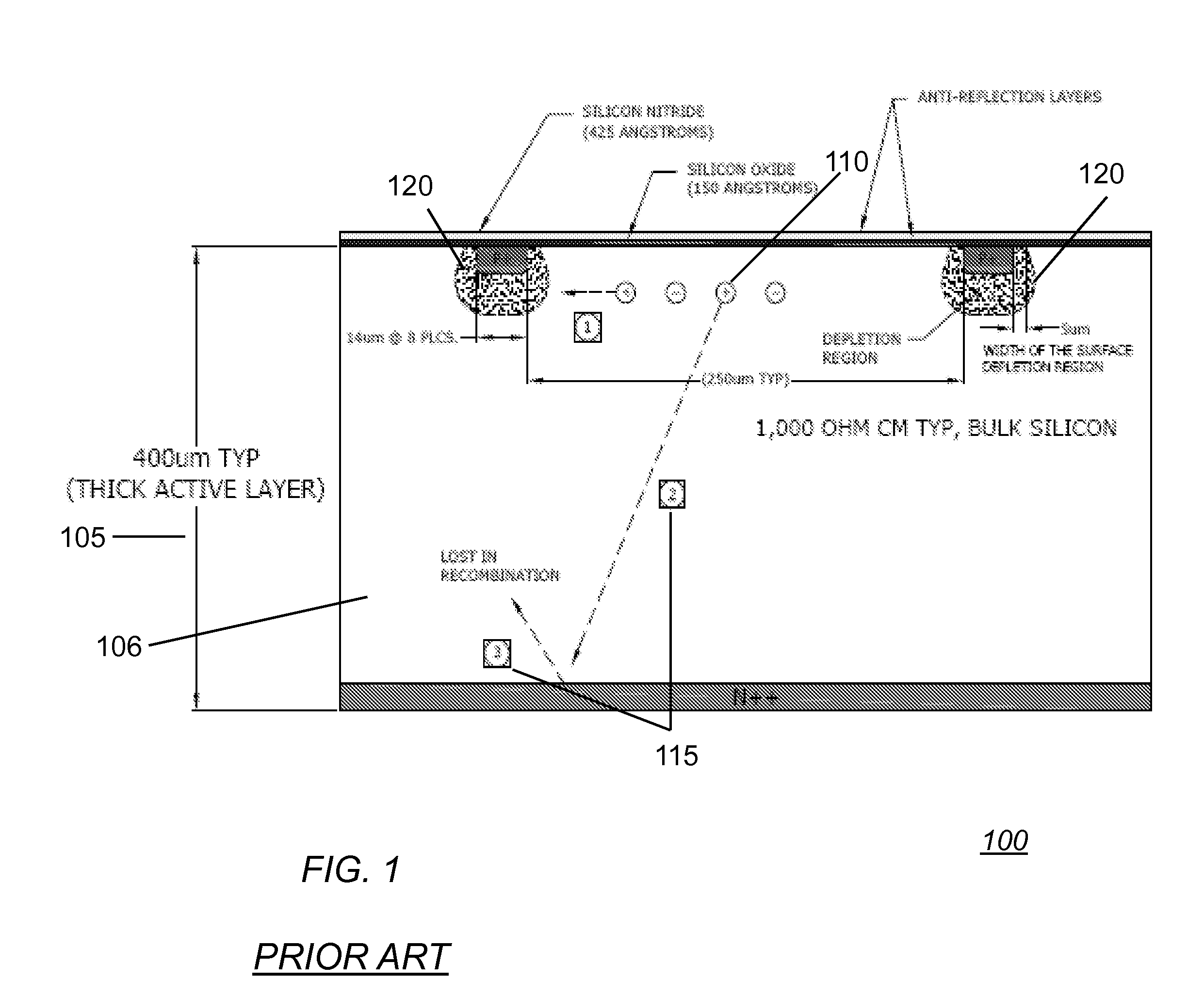
In addition, the fishbone photodiode device in the prior art as shown in FIG. 1 is disadvantageous because the high volume, thick
active layer 105 that is used to fabricate the photodiode results in high dark current, since dark current is proportional to the overall volume of the
active layer of the device.
In addition, the conventional photodiode array described above with respect to FIG. 1 is disadvantageous in that the photodiode tends to degrade in shunt resistance since the P-N junction is passivated by relatively thin antireflective
layers, such as
silicon oxide on the order of 150 Å and
silicon nitride on the order of 425 Å.
The result is a fishbone photodiode having high noise characteristics, and thus, a poor
signal to noise ratio.

