Nitride semiconductor laser device and fabrication method thereof

Inactive Publication Date: 2008-12-11
SHARP KK
View PDF5 Cites 18 Cited by
  • Summary
  • Abstract
  • Description
  • Claims
  • Application Information

AI Technical Summary

Benefits of technology

[0023]According to the present invention, near the end surface of the resonator, the etched-in portion can stop a step which begins to appear on the end surface of the resonator during cleaving. Accordingly, it is possible to prevent the step from developing at the stripe-shaped waveguide where laser light is emitted. In this way, it is possible to prevent damage to the end surface of the laser emission portion, and it is thus possible to fabricate a nitride semiconductor laser device that can emit laser light with satisfactory reliability even after being driven for a long time.
[0024]Moreover, according to the invention, the reduced influence of the Stark effect an

Problems solved by technology

Disadvantageously, however, the conventional nitride semiconductor laser device, the nitride semiconductor layers of which are laminated on a nitride semiconductor substrate (hereinafter, called an “a-surface nitride semiconductor substrate”) having the (11-20) plane as the principal plane with a typical process of photolithography, vacuum deposition, polishing, cleaving and coating, does not offer satisfactory characteristics to ensure its reliability.
That is, when conventional nitride semiconductor devices are subjected to CW (continuous wave) oscillation (continuous oscillation) up to a high output, a certain percentage of them are damaged before reaching the point where they output enough light.
Moreover, the longer the time for driving the conventional nitride semiconductor laser devices is, the higher the percentage of the damaged deices becomes.
Depending o

Method used


Image

  • Nitride semiconductor laser device and fabrication method thereof
  • Nitride semiconductor laser device and fabrication method thereof
  • Nitride semiconductor laser device and fabrication method thereof

Examples


Example

Embodiment 1

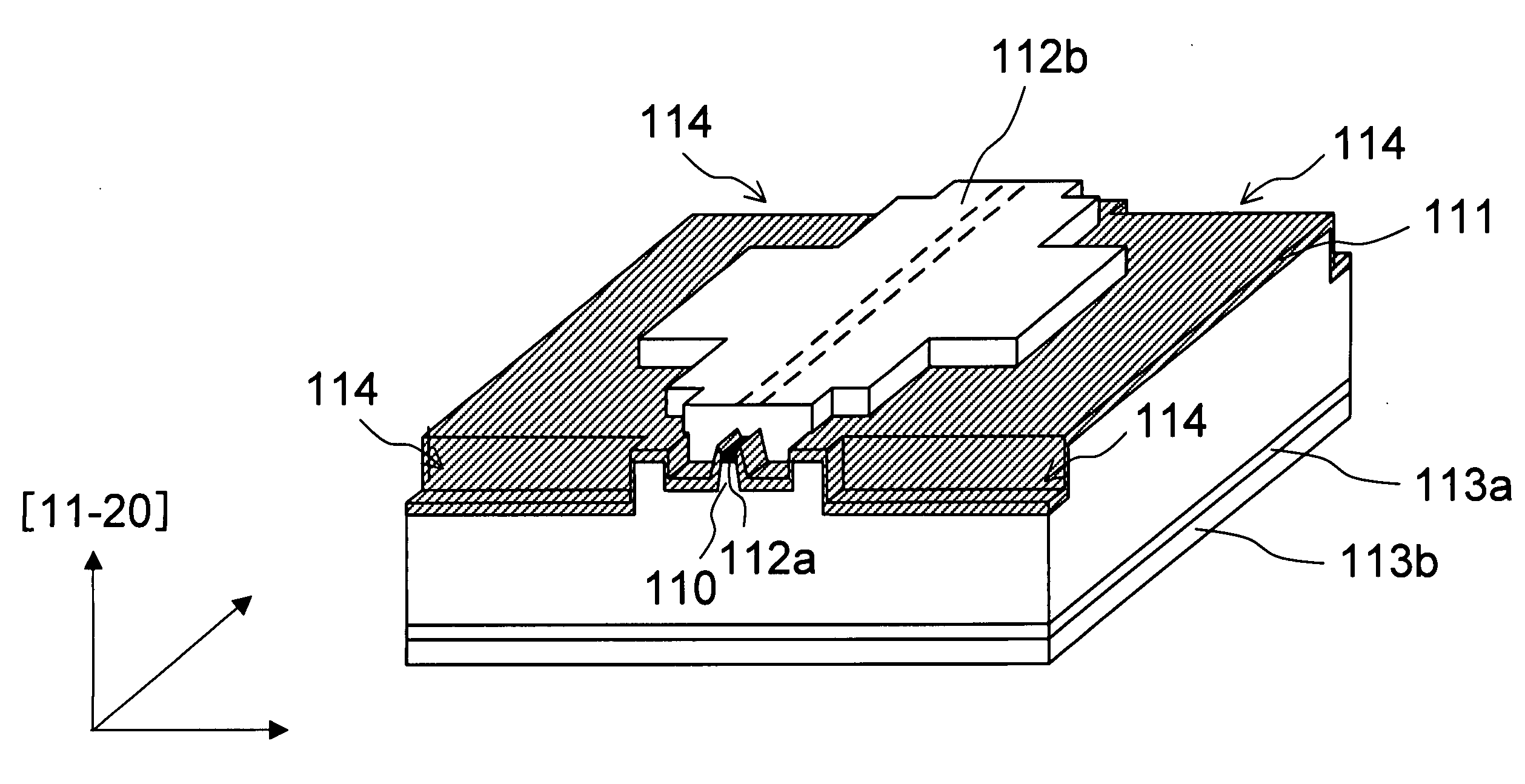
[0084]By use of the [0001] direction (c-axis direction) as the direction in which the striped-shape resist is formed on the p electrode 112a and each process described above, the nitride semiconductor laser device 100 according to this embodiment is made. As shown in FIG. 12, the resist mask 122 to form the etched-in portion 114 is provided with the stripe-shaped opening portions 123 that are formed at equal intervals in both [0001] direction (c-axis direction) and [1-100] direction (m-axis direction) as shown in FIG. 3. The rectangular openings 123 are formed on the scribe lines extending in the [1-100] direction (m-axis direction) in which the wafer is cleaved into the bars to obtain the mirror surfaces (resonator end surfaces).

[0085]In the forming process of the mirror surface in this embodiment, because the ridge stripe is formed in the [0001] direction (c-axis direction) of the GaN substrate 101 having (11-20) plane as its principal plane, the (0001) plane (c plane...

Example

[0086]In the same way as in the first embodiment, by use of the [0001] direction (c-axis direction) as the direction in which the striped-shape resist is formed on the p electrode 112a and each process described above, the nitride semiconductor laser device 100 according to this embodiment is also made. Accordingly, the (0001) plane (c plane) is used as the cleavage surface of the nitride semiconductor laser device 100. Specifically, the resist mask 122 to form the etched-in portion 114 is provided with the stripe-shaped opening portions 123 as shown in FIG. 14 that extend in the [0001] direction (c-axis direction) and are formed at equal intervals in the [1-100] direction (m-axis direction) as shown in FIG. 4.

[0087]In this embodiment, the stripe-shaped etched-in regions 114 each having a width of 70 μm are formed on both sides of and in parallel with the ridge stripe 110 at the positions away from the center of the 20-μm-wide stripe which has the ridge stripe 110 at its center. Acc...

Example

Embodiment 3

[0088]Unlike the first embodiment, the nitride semiconductor laser device 100 is made by use of the [1-100] direction (m direction) in which the stripe-shaped resist is formed on the p electrode 112a and each process described above. The resist mask 122 to form the etched-in portion 114 is provided with the stripe-shaped opening portions 123 as shown in FIG. 16 that are formed at equal intervals in both [0001] direction (c-axis direction) and [1-100] direction (m-axis direction) as shown in FIG. 3. The rectangular openings 123 are formed on the scribe lines extending in the [0001] direction (c-axis direction) in which the wafer is cleaved into the bars to obtain the mirror surfaces (resonator end surfaces).

[0089]In the forming process of the mirror surface in this embodiment, because the ridge stripe is formed in the [1-100] direction (m-axis direction) of the GaN substrate 101 having (11-20) plane as its principal plane, the (1-100) plane (m plane) is used as the cleava...


PUM


Abstract

In a nitride semiconductor laser device so structured as to suppress development of a step on nitride semiconductor layers, the substrate has the (11-20) plane as the principal plane, the resonator end surface is perpendicular to the principal plane, and, in the cleavage surface forming the resonator end surface, at least by one side of a stripe-shaped waveguide, an etched-in portion is formed as an etched-in region open toward the surface of the nitride semiconductor layers.

Description

[0001]This nonprovisional application claims priority under 35 U.S.C. §119(a) on Patent Application No. 2007-150639 filed in Japan on Jun. 6, 2007, the entire contents of which are hereby incorporated by reference.BACKGROUND OF THE INVENTION[0002]1. Field of the Invention[0003]The present invention relates to a nitride semiconductor laser device and to a method for fabricating it. More particularly, the invention relates to a nitride semiconductor laser device having nitride semiconductor layers laminated on a nitride semiconductor substrate having a particular planar orientation, and to a method for fabricating such a nitride semiconductor laser device.[0004]2. Description of Related Art[0005]Nitride semiconductors are compounds of N (nitrogen), which is a group V element, and a group III element, such as Al (aluminum), Ga (gallium), and In (indium). Because of their band structures and chemical stability, nitride semiconductors have been receiving much attention as semiconductor m...

Claims


Application Information

Patent Timeline
IPC IPC(8): H01S5/026H01L21/02
CPCB82Y20/00H01S5/0202H01S5/0425H01S5/22H01S5/2201H01S5/2214H01S5/3202H01S5/34333H01S2301/173H01S5/04254H01S5/32025
Inventor YAMAMOTO, SHUICHIROITO, SHIGETOSHIYAMASHITA, FUMIOKAWAKAMI, TOSHIYUKI
Owner SHARP KK
Why Eureka
Try Eureka