Display device and method for manufacturing the same

a technology of a display device and a manufacturing method, which is applied in the field of display devices, can solve the problems of large power consumption, short half-life of luminescence, and insufficient luminance of a conventional light-emitting element, and achieve the effects of reducing current efficiency, reducing the ratio of injected holes to light emission, and improving the effect of injection holes

Inactive Publication Date: 2009-02-12
SEMICON ENERGY LAB CO LTD
View PDF52 Cites 23 Cited by
  • Summary
  • Abstract
  • Description
  • Claims
  • Application Information

AI Technical Summary

Benefits of technology

[0011]In view of the above problem, an object of the present invention is to provide a display device having favorable luminescence property, achieving brightness with lower power consumption, and having high stability.
[0024]The following advantageous effect is obtained as a hole injection electrode by applying a laminated structure of the conductive transparent oxide layers containing silicon or silicon oxide and by containing silicon or silicon oxide of high concentration in a conductive layer on the side of an organic compound and containing silicon or silicon oxide of low concentration in the other conductive layer. That is, an original advantageous effect of work function of a hole injection electrode is obtained by providing a conductive layer containing silicon or silicon oxide of high concentration on the side of an organic compound layer; therefore, hole injection efficiency to a hole injection layer is increased and a luminescence property can be improved. In addition, resistivity of a hole injection electrode can be controlled low by providing a conductive layer containing silicon or silicon oxide of low concentration as the other conductive layer.
[0025]Here, a mechanism in which hole injection efficiency to a hole injection layer is improved by applying the conductive transparent oxide layer containing silicon or silicon oxide as a hole injection electrode as follows.
[0026]FIG. 3 shows a band scheme showing a contact of a conventional conductive transparent oxide (CTO) layer and a hole injection layer (HIL). When the contact is not formed properly, a band of a hole injection layer is warped in a direction that makes a barrier against an electron due to an effect of an interface potential, and a hole is stored in vicinity of the interface. The conductive transparent oxide film changes in a direction of which work function is low depending on a polluted state of the surface or the like. In such a case, injection of a hole decreases and a ratio that the injected hole contributes to light emission is decreased; therefore, current efficiency decreases.
[0027]On the other hand, in FIGS. 4A and 4B, a conductive transparent oxide layer of high silicon oxide concentration (CTO2) is provided adjacent to an HIL. Furthermore, the figures shows a band scheme in the case of a layer obtained by precipitating silicon (Si), silicon oxide (SiOx), silicon nitride (SiNx), silicon oxynitride (SiOxNy), silicon nitride oxide (SiNxOy), or the like in a step of forming a light-emitting element or a layer obtained by intentionally depositing silicon, silicon oxide, silicon nitride, and the like by a vapor deposition method or a sputtering method on the surface or inside a layer in vicinity of the surface (referred to as a “barrier layer”). In this case, a band is flattened as shown in FIG. 4A, or the band is bended below as shown in FIG. 4B so that the hole does not accumulate between the hole injection electrode and the HIL. Therefore, injection of a hole is improved and an advantageous effect of increasing a ratio that an injected hole contributes to light emission can be obtained.

Problems solved by technology

However, adequate luminance is not obtained in a conventional light-emitting element, that is, a light-emitting element having a structure in which an organic compound is sandwiched between an anode made from ITO or the like and a cathode made from MgAg, Al, and the like.
In addition, power consumption is large and half-life time of luminescence is short in the conventional light-emitting element; therefore, there is a problem to be solved in respect of stability.

Method used


Image

  • Display device and method for manufacturing the same
  • Display device and method for manufacturing the same
  • Display device and method for manufacturing the same

Examples


embodiment 1

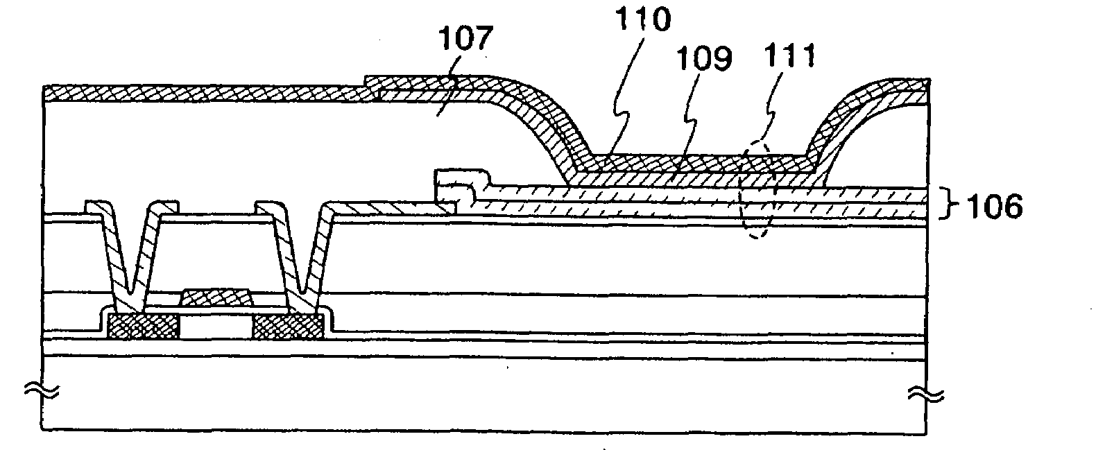
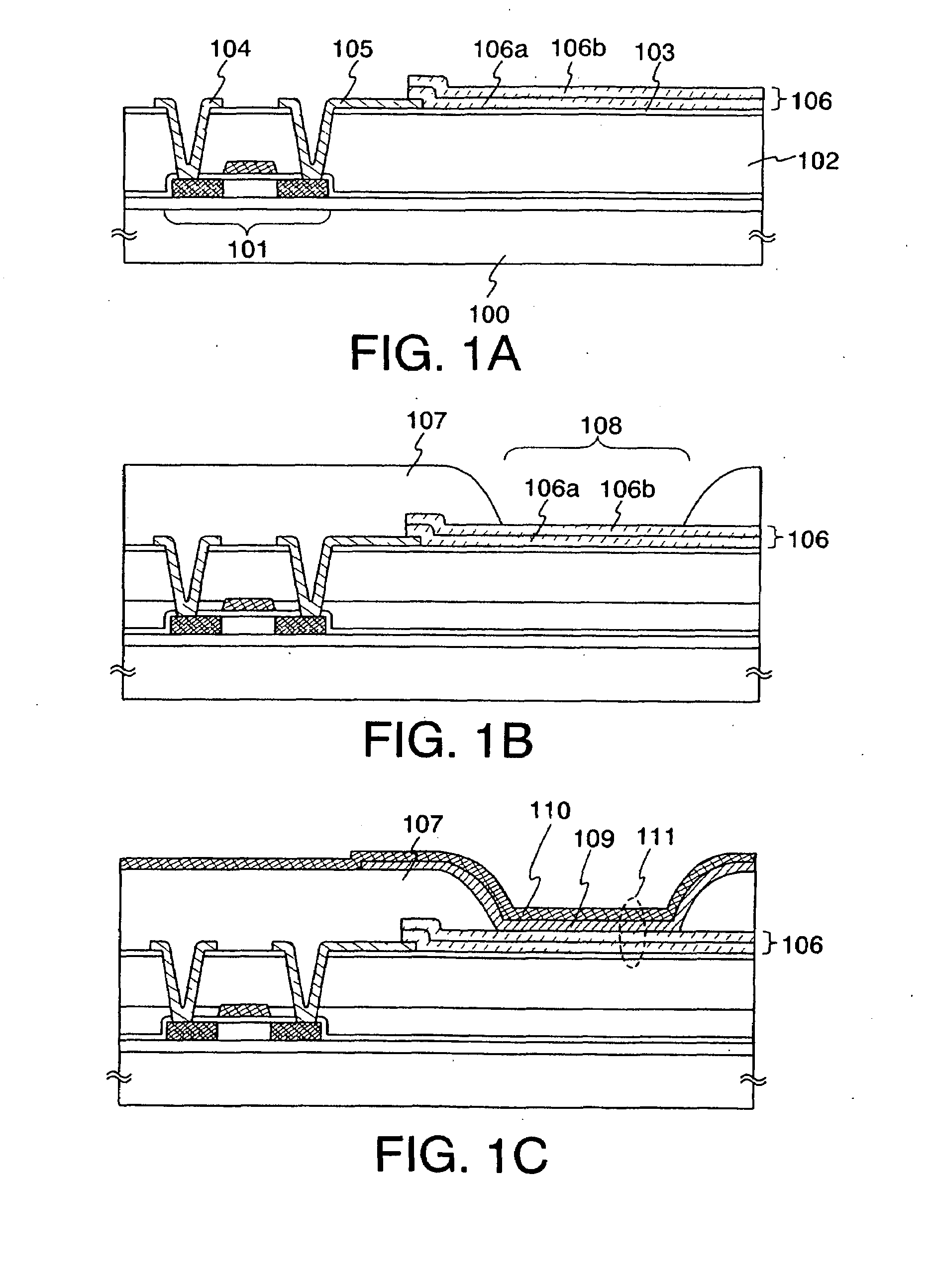
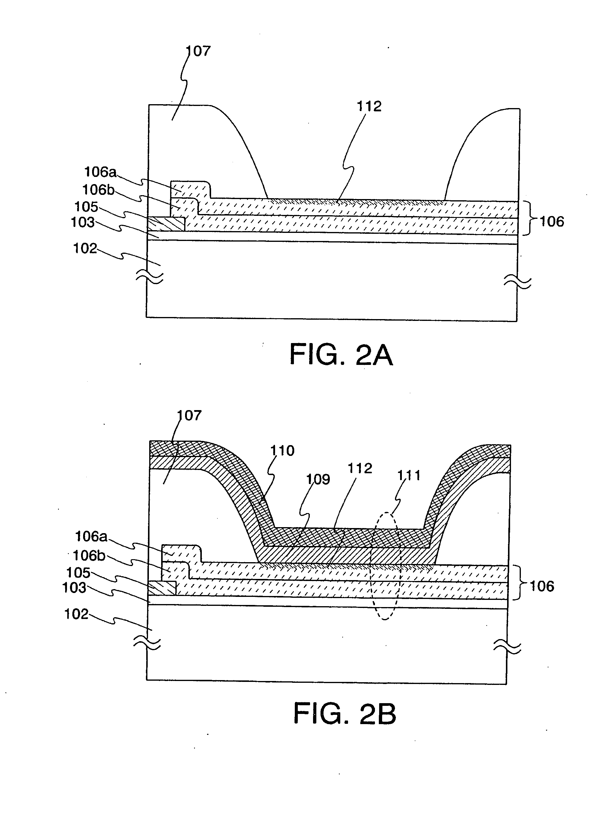
[0076]Embodiments of a light-emitting element concerning the present invention are specifically described with reference to FIGS. 7A to 7C, 8A and 8B.

[0077]In this embodiment, the case in which the invention is applied to an active matrix display device, in which a pixel portion and a driver circuit portion are formed over one substrate, is described

[0078]First, a base insulating film 601 is formed on a substrate 600. A glass substrate, a quartz substrate, a silicon substrate, a metal substrate (Al or the like), a stainless substrate, a plastic substrate that has heat resistance withstanding a processing temperature of a manufacturing process, or the like can be used for the substrate 600. Note that when a plastic substrate that is transformed by a processing temperature of a manufacturing process is used, a method for forming TFTs 607, 609, and 610 preliminary over another substrate (a glass substrate, a quartz substrate, or the like) and transferring them to a plastic substrate th...

embodiment 2

[0120]The case to which the present invention is applied in a bottom emission type light-emitting device shown in FIG. 9B is described in Embodiment 1. The case to which the invention is applied in a top emission type light-emitting device shown in FIG. 9A and a dual emission type light-emitting device shown in FIG. 9C is described in this embodiment.

[0121]First, the case of the dual emission type light-emitting device is described. In this case and Embodiment 1 alike, as a material of a hole injection electrode, conductive transparent oxide layer, containing silicon or silicon oxide, such as ITO, zinc oxide (ZnO), or IZO can be used by laminating. It is preferable to use ITSO containing silicon or silicon oxide of which concentration ranges from 0% to 20 atomic % and further to use a lamination of an ITSO layer containing silicon or silicon oxide of a low concentration (more preferably, from 1 atomic % to 6 atomic %) and an ITSO layer containing silicon or silicon oxide of a high c...

embodiment 3

[0126]The case applying the present invention to an active matrix type light-emitting device having a reverse stagger structure is described in this embodiment with reference to FIGS. 10A-10D and 11.

[0127]A conductive film for forming a gate electrode and a gate wiring (a scanning line) is formed over a substrate 1100 made from the same material as that of Embodiment 1. A metal material such as chromium, molybdenum, titanium, tantalum, tungsten, or aluminum or the alloy material thereof is used for the conductive film. This conductive film can be formed by a sputtering method and a vapor deposition method.

[0128]A conductive film is etched to form gate electrodes 1101 and 1102. Since a first semiconductor film and a wiring layer are formed over the gate electrodes 1101 and 1102, it is preferable that the conductive film is processed so that the edge thereof has a taper shape. When the conductive film is formed from a material containing aluminum as the main component, the surface may...


PUM

PropertyMeasurementUnit
temperaturesaaaaaaaaaa
curvature radiusaaaaaaaaaa
temperaturesaaaaaaaaaa

Abstract

According to one aspect of the present invention, a laminated structure of conductive transparent oxide layers containing silicon or silicon oxide is applied as an electrode on the side of injecting a hole (a hole injection electrode; an anode) instead of the conventional conductive transparent oxide layer such as ITO. In addition, according to another aspect of the invention, a laminated structure of conductive transparent oxide layers containing silicon or silicon oxide, each of which content is different, is applied as a hole injection electrode. Preferably, silicon or a silicon oxide concentration of the conductive layer on the side where it is connected to a TFT ranges from 1 atomic % to 6 atomic % and a silicon or silicon oxide concentration on the side of a layer containing an organic compound ranges from 7 atomic % to 15 atomic %.

Description

CROSS-REFERENCE TO RELATED APPLICATIONS[0001]This application is a divisional of U.S. application Ser. No. 10 / 937,904, filed Sep. 10, 2004, now allowed, which claims the benefit of a foreign priority application filed in Japan as Serial No. 2003-329201 on Sep. 19, 2003, both of which are incorporated by reference.BACKGROUND OF THE INVENTION[0002]1. Field of the Invention[0003]The present invention relates to a display device utilizing a conductive transparent oxide layer as an electrode. Specifically, an object of the invention is to improve a light-emitting element in a luminescence property, to improve resistivity of an electrode, and to reduce power consumption of a display device by controlling a concentration of silicon or silicon oxide in the conductive layer.[0004]2. Description of the Related Art[0005]A light-emitting element formed by mainly sandwiching a material that emits electroluminescence (hereinafter referred to as “EL”) made from an organic compound between a pair o...

Claims


Application Information

Patent Timeline
Patent Type & Authority Applications(United States)
IPC IPC(8): H01L33/00G09F9/30H01L27/32H01L51/50H01L51/52H05B33/10H05B33/26H05B33/28
CPCH01L27/3244H01L27/3281Y10S428/917H01L51/5206H01L27/3295H10K59/122H10K59/17H10K50/816H10K50/81H10K59/12
Inventor YAMAZAKI, SHUNPEITAKAYAMA, TORUSAKAMOTO, NAOYAAKIMOTO, KENGOSATO, KEIJIMARUYAMA, TETSUNORI
Owner SEMICON ENERGY LAB CO LTD
Why Eureka
Try Eureka