Eureka AIR delivers breakthrough ideas for toughest innovation challenges, trusted by R&D personnel around the world.

Method for fabricating minute conductive structures on surfaces

Inactive Publication Date: 2009-03-05
CLARIANT INT LTD +1
View PDF9 Cites 17 Cited by
  • Summary
  • Abstract
  • Description
  • Claims
  • Application Information

AI Technical Summary

Benefits of technology

[0017]However, the parameters of pressure, temperature and duration of pressing correlate such that, at higher temperature or greater pressure, the pressing time can be reduced. As a result, correspondingly shorter times and thus higher component throughput rates are conceivable with the method presented here. Furthermore, methods that show the desired result using high pressures and short duration even at correspondingly low temperature of dies or rollers are thus also conceivable.
[0023]In a preferred variation, movable pressure heads are provided, which follow the stamped channel structure during the relative movement of the substrate under them. For example, this is the case when curved, preferably corrugated channels have been stamped along the orientation of the substrate. When the pressure heads can move at right angles to the flow-through direction of the substrate, an oscillation in the pressure heads in a perpendicular direction to the substrate relative to the latter leads to a wave movement. Hence, a corrugated structure can be continuously filled with ink. Particularly with interrupted structures, this can be extended to assemblies, where the pressure heads follow the flow-through direction of the substrate for a short time. This means that a pressure head device is provided that permits movement in two dimensions.
[0025]Polymer materials frequently have special properties, that make them preferred materials in many fields of application. This comprises, for example, their comparatively high flexibility, the frequently lower density with identical or similar load carrying capacity in comparison to anorganic materials and the wide design freedom due to the easier mouldability of these materials. Some materials (e.g. polycarbonate, polypropylene, polymethyl methacrylate (PMMA) and some PVC types) simultaneously display additional special properties, such as, for example, optical transparency. Preferred polymers to be used in the present method are transparent and / or have a high glass transition temperature. Polymers with a high glass transition temperature refers to polymers with a glass transition temperature above 100° C. Particularly preferred polymers to be used in the present method are selected from the group consisting of polycarbonate, polyurethane, polystyrene, polymethyl(meth)acrylate and polyethylene terephthalate.
[0029]If the suspensions of metal nanoparticles in solvents as described above are used in another preferred variation of the method, then the after-treatment consists of heating the complete component or just the conductor paths to a temperature, at which the metal particles sinter together and the solvent at least partially evaporates. In this arrangement, metal particles with the smallest possible particle diameter are advantageous, as the sinter temperature is proportional to the particle size in nanoscale particles, so that the sinter temperature required for smaller particles is lower than for larger ones. In this arrangement, the boiling point of the solvent is as near as possible to the sintering temperature of the particles and is as low as possible, in order to protect the substrate from thermal effects. A preferred ink solvent to be used is one with a boiling temperature of <250° C., particularly preferred with a temperature <200° C., particularly with a temperature ≦100° C. All temperatures given here refer to boiling temperatures at a pressure of 1013 hPa. Particularly preferred solvents are n-alkanes with up to 12 carbon atoms, alcohols with up to four carbon atoms, such as for example, methanol, ethanol, propanol and butanol, ketones and aldehydes with up to five carbon atoms, such as for example acetone and propanal, water, as well as acetonitrile, dimethyl ether, dimethyl acetamide, dimethyl formamide, N-methyl-pyrrolidone (NMP), ethylene glycol and tetrahydrofuran. The sintering stage is carried out at the given temperature until a continuous conductor path is formed. A preferred duration for sintering is from one minute to 24 hours, particularly preferred from five minutes to 8 hours, particularly preferred from two to 8 hours.

Problems solved by technology

Furthermore, there is a need to equip the surfaces with such structures that cannot be seen by the naked eye, if possible, without the surface's transparency, translucence and lustre, for example, being negatively influenced.
This solution cannot be put into practice, as reducing the diameter means the rheological limits of the printing substances used (varnishes, inks, conductor pastes, etc.) start to dominate.
This often makes the printing substances unusable for the application.
Particular complications possible here are due to the jet blocking, as the printing substance contains dispersed particles.
Furthermore, the rheological requirements (determined viscosity and surface tension, as well as contact angle and wetting of the substrate) cannot be adjusted independently of each other, so that an ink, which is still printable with such a jet, does not display the desired properties in the printed image on the substrate.
Alternative, commercial printing technologies, such as offset or screen printing, are generally not able to apply such minute structures onto a surface.
These methods, however, do require labour-intensive lithographic stages.
This process is relatively difficult and labour-intensive due to the many treatment stages.
The disadvantage of this method is that, besides the potential high losses of filling material, it is very difficult to ensure that the substrate is completely free of residues of the filling material in places not to be filled.
However, filling such structures with material, that is subsequently made conductive, has not yet been published.

Method used


Image

  • Method for fabricating minute conductive structures on surfaces
  • Method for fabricating minute conductive structures on surfaces

Examples


example 1

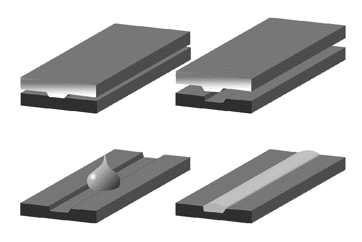
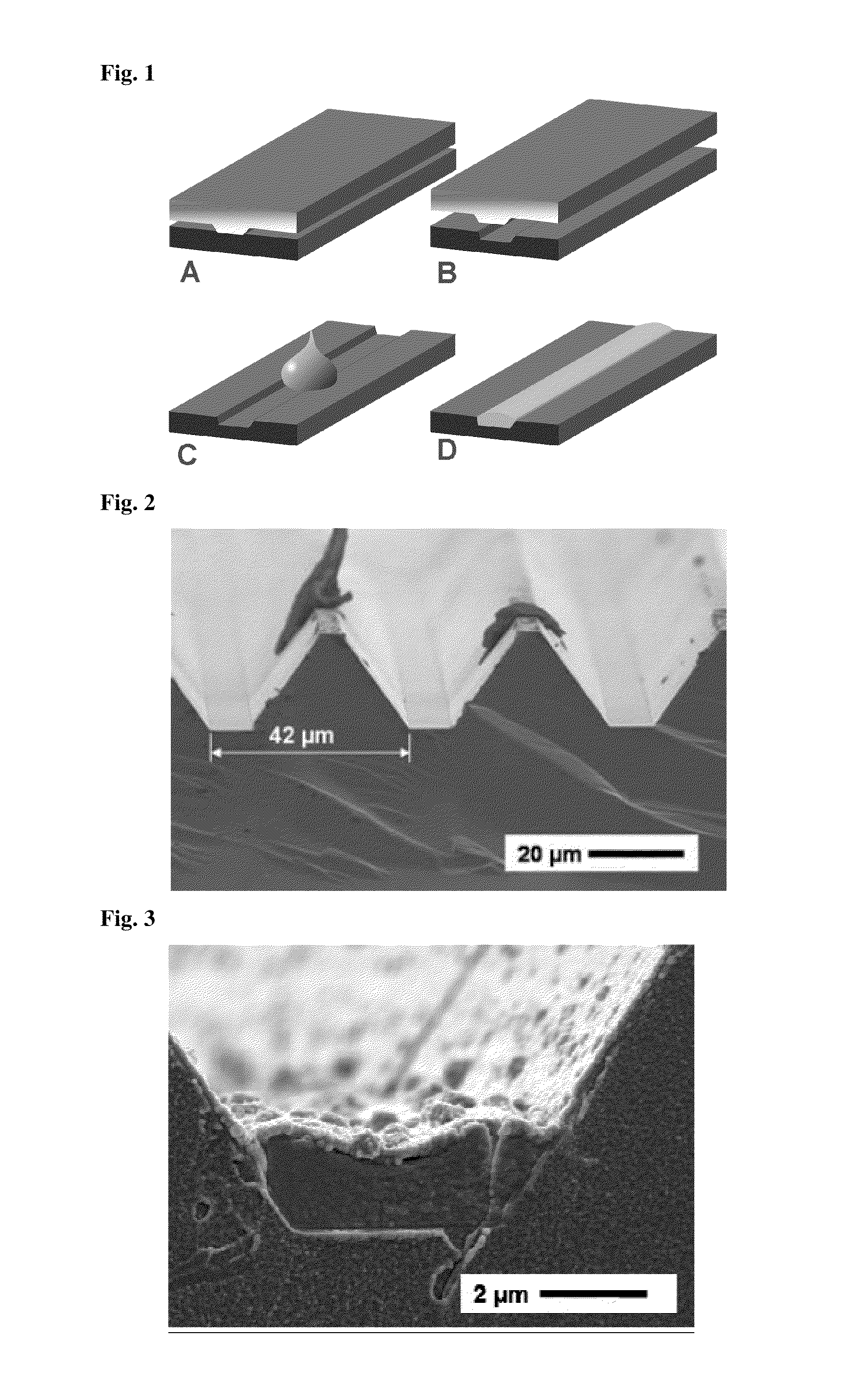
[0035]A grid of channels on a polymer substrate has been fabricated by pressing a grid structure (MASTER) into a polystyrene substrate with a glass transition temperature Tg of 100° C. (N5000, Shell AG). For this purpose, the MASTER was heated to 180° C. and pressed onto the substrate for 3 minutes with a load of 3 kg by means of a small press (Tribotrak, DACA Instruments, Santa Barbara, Calif., USA). The MASTER displayed a line interval of 42 μm, the depressions in the MASTER, when viewed in cross-section, appearing as cut-off triangles standing on their heads (FIG. 2). The elevations in the MASTER display a height of 20 μm and are also cut-off triangles when viewed in cross-section. The base width of the elevations in the MASTER was 32 μm and the width at the peak of the elevations approximately 4.5 μm.

[0036]A single droplet of a silver nano-ink (Nanopaste™, Harima Chemicals, Japan) was placed on one of the lines fabricated as described above. The ink consists of a dispersion of s...

example 2

[0037]A grid of channels was created by pressing a grid into a polycarbonate film with a glass transition temperature Tg of 205° C. (Bayfol®, Bayer MaterialScience AG), which was heated to 270° C. All further stamping parameters corresponded to Example 1. In the same way as in Example 1, a conductive line was also created. The line width achieved and lengths of electrically conductive silver conductor paths were identical to those of the paths created in Example 1.

example 3

[0038]The method was the same as in Example 1, but a press roller was used instead of the stamping method with a press die.

[0039]Continuous structures on a 10 mm thick polycarbonate substrate (Makrolon, Bayer, Germany, glass temperature 148° C.) were created by means of a roller mounted on a small press (Tribotrak, DACA Instruments, Santa Barbara, Calif., USA). The specially finished roller, mounted on the small press, possessed raised line structures with a width of 10 μm and an interval of 3 mm. In this arrangement, the surface of the substrate was heated to 60° C., while the roller had a temperature of 155° C. The pressure of the press was set on the assembly mentioned above by means of a weight of 10 kg. A relative drive speed from roller to substrate of 0.25 mm / s was selected for the temperatures set and the pressure used. In this arrangement, the substrate was pulled along under the roller by means of a slide, in order to achieve the relative speed indicated above. The pressur...


PUM


Abstract

Method for producing small and micro conductive structures on surfaces by (hot) stamping and / or nanoscale imprinting microstructures on the surfaces, targeting conductive material into the channels thus created with the aid of capillary action, and appropriately after-treating the conductive material.

Description

[0001]The present invention pertains to a method that enables small and micro conductive structures to be fabricated on surfaces. In this context, small and micro structures are structures that generally can only be seen by the naked eye with the help of optical aids. This is achieved by fabricating micro-channels by (hot) stamping and / or imprinting nanoscale depressions, subsequent targeted introduction of conductive material into the depressions thus created, assisted by the physical effect of capillary action, and finally suitable after-treatment of the conductive material.BACKGROUND OF THE INVENTION[0002]There is a need to equip the surfaces particularly of electrically non-conductive or poorly conductive transparent objects with electrically conductive structures, without thereby affecting their optical or mechanical and physical properties. Furthermore, there is a need to equip the surfaces with such structures that cannot be seen by the naked eye, if possible, without the sur...

Claims


Application Information

Patent Timeline
IPC IPC(8): B32B5/00B05D5/12
CPCH05K1/097H05K3/0014H05K3/107H05K3/125Y10T428/26H05K2201/0108H05K2203/0108H05K2203/013H05K3/1258H01L21/027
Inventor BAHNMULLER, STEFANEIDEN, STEFANIEMEIER, STEPHAN MICHAELHENDRIKS, CHRISTIAN ETIENNESCHUBERT, ULRICH
Owner CLARIANT INT LTD
Why Eureka
Eureka Blog
Learn More