

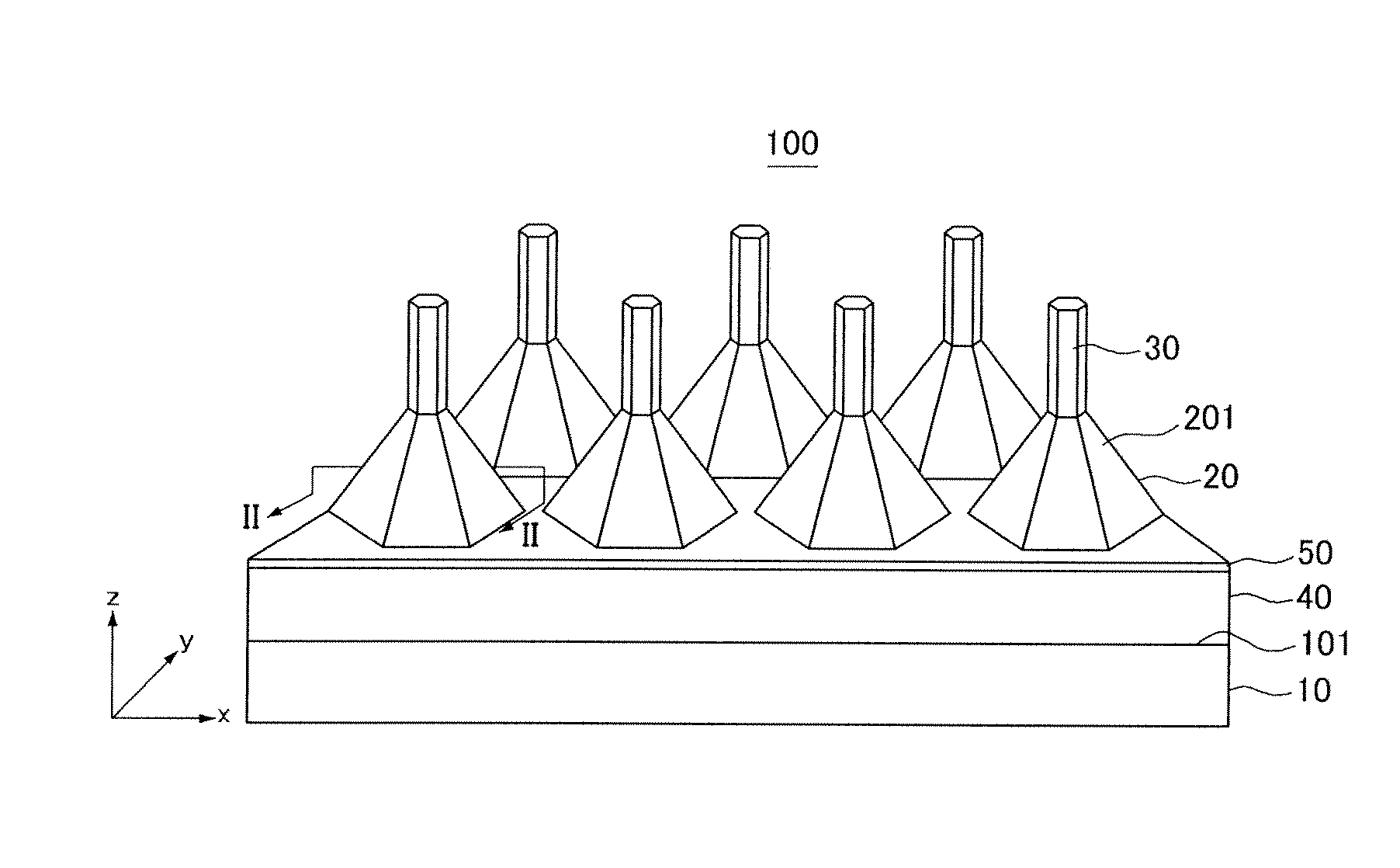
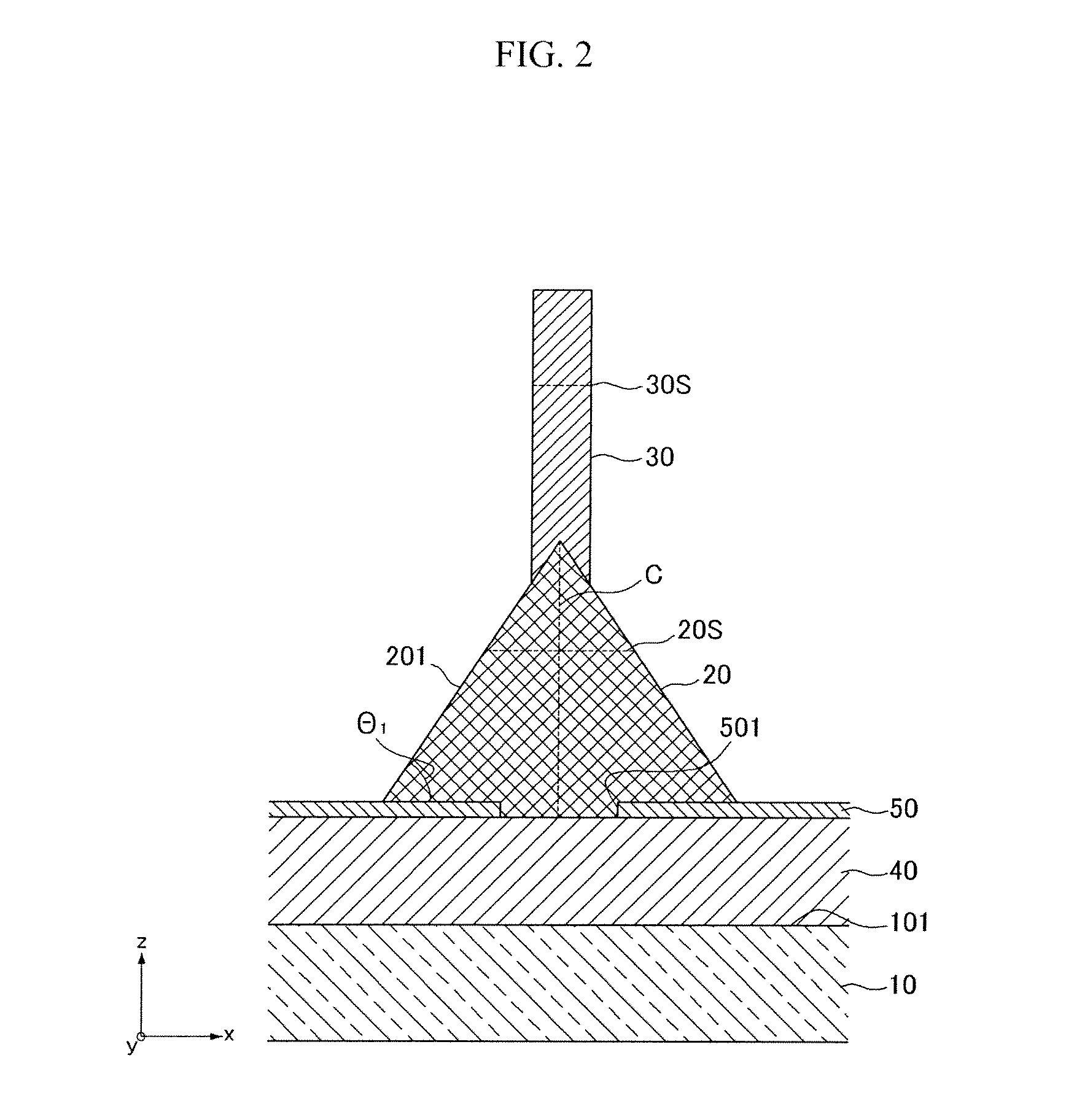
Nanodevice Comprising a Nanorod and Method for Manufacturing the Same
a nano-rod and nano-technology, applied in the field of nano-rods, can solve the problems of difficult to form a nano-rod with a uniform diameter and length, the conventional manufacturing technique of semiconductor nano-rods, and the inability to freely control electric conductivity, etc., to achieve the effect of enhancing the integration degree of the nano-rod, high purity, and large amount of nano-rods
- Summary
- Abstract
- Description
- Claims
- Application Information
AI Technical Summary
Benefits of technology
Problems solved by technology
Method used
Image


Examples
exemplary example 1
[0095]The seed layer was formed on the substrate. The seed layer made of gallium nitride was formed on the substrate made of a silicon single crystal by using metal organic chemical vapor deposition (MOCVD).
[0096]Next, amorphous silicon oxide SiO2 or silicon nitride SiNx was deposited on the seed layer to pattern the seed layer. In this case, the method of plasma-enhanced chemical vapor deposition was used.
[0097]As a result, a mask layer with the thickness of about 50 nm was formed on the seed layer. A photosensitive resin was baked after it was formed on the mask layer by using a spin coating method. Polymethyl methacrylate (PMMA) was used as a material of the photosensitive resin.
[0098]The photosensitive resin was formed on the mask layer and was then heated. In addition, the photosensitive resin was exposed to a light or an electron beam with a predetermined pattern. Next, a portion of the photosensitive resin that was only exposed to the light was removed by etching with a devel...
exemplary example 2
[0120]A nanodevice was manufactured by using a method that is the same as that of the above-described Exemplary Example 1, except for the temperature for forming a nanorod in the organic metal chemical vapor deposition reactor. A crystal with a hexagonal column shape was manufactured by maintaining a temperature of a range of about 800° C. to 1000° C. in the organic metal chemical vapor deposition reactor. Not only a crystal with a hexagonal column shape but also a crystal with a hexagonal cone shape can be obtained.
[0121]FIG. 27 shows a tilt-view scanning electron microscopy photograph of a crystal manufactured according to a second Exemplary Example of the present invention. As shown in FIG. 27, a plurality of crystals, which are spaced apart from each other, can be manufactured. Each of the crystals has a hexagonal column shape.
[0122]FIG. 28 shows a scanning electron microscopy photograph of a cross-section of a crystal of FIG. 27. As described in FIG. 28, each of the crystal has...
PUM
| Property | Measurement | Unit |
|---|---|---|
| angle | aaaaa | aaaaa |
| angle θ1 | aaaaa | aaaaa |
| angle | aaaaa | aaaaa |
Abstract
Description
Claims
Application Information