Variable resistance element, its manufacturing method and semiconductor memory device comprising the same

a technology of variable resistance and manufacturing method, which is applied in the direction of semiconductor devices, solid-state devices, instruments, etc., to achieve the effects of stable resistance switching operation, favorable data retention characteristics, and stable switching operation

Inactive Publication Date: 2009-04-16
SHARP KK
View PDF5 Cites 44 Cited by
  • Summary
  • Abstract
  • Description
  • Claims
  • Application Information

AI Technical Summary

Benefits of technology

[0024]When the variable resistor is formed of titanium oxide or titanium oxynitride having the crystal grain diameter of 30 nm or less, the variable resistance element can implement the stable switching operation and favorable data retention characteristics.
[0025]Especially, according to the above constitution, since the crystal state of the variable resistor is changed and as a result, the resistance value is changed in response to the application of the voltage pulse, the forming process is not needed and the stable resistance switching operation can be provided. In addition, since the resistance switching operation is not performed by the filament path, the resistance fluctuation is small even after the switching is repeated, and the resistance fluctuation is small even after held over a long period at high temperature. Therefore, the element of the present invention is advantageously applied to a nonvolatile memory.
[0026]In addition, according to the constitution of the present invention, since the resistance switching operation is not performed by the filament path as described above, area dependency is provided by miniaturizing the resi

Problems solved by technology

However, the above memory devices at the present have both merits and demerits and an ideal “uni

Method used


Image

  • Variable resistance element, its manufacturing method and semiconductor memory device comprising the same
  • Variable resistance element, its manufacturing method and semiconductor memory device comprising the same
  • Variable resistance element, its manufacturing method and semiconductor memory device comprising the same

Examples


first embodiment

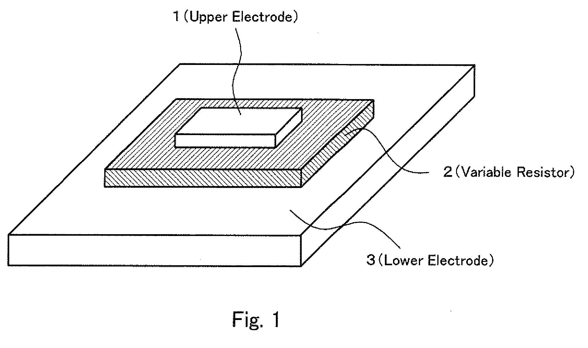
[0103]A first embodiment (referred to as “this embodiment” occasionally hereinafter) of the element of the present invention and its manufacturing method will be described with reference to FIGS. 1 to 19. In addition, the element of the present invention is characterized by a material used for a variable resistor serving as one component and its overall constitution is the same of the variable resistance element having the conventional constitution described in the section of the background art as shown in FIG. 1.

[0104]According to the element of the present invention in this embodiment, a variable resistor 2 contained in the variable resistance element shown in FIG. 1 is formed of titanium oxide having a grain diameter of 30 nm or less as will be described below.

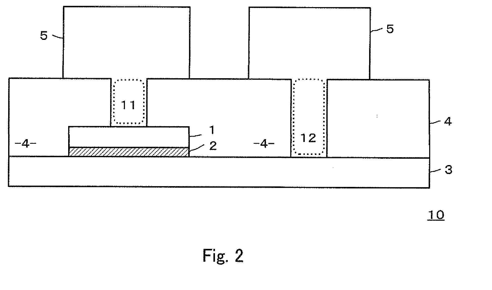
[0105]FIG. 2 is a schematic section view showing the element of the present invention in this embodiment. An element 10 of the present invention comprises a lower electrode 3, the variable resistor 2, an upper electrode 1 l...

second embodiment

[0148]A description will be made of an element of the present invention and its manufacturing method according to a second embodiment (referred to as “this embodiment” occasionally hereinafter). According to this embodiment, a variable resistor 2 is formed of titanium oxynitride in which one part of oxygen of anatase-type titanium oxide is replaced with nitride, so that only step S2 for depositing a variable resistor film is different from the manufacturing method of the first embodiment shown in FIG. 10.

[0149]That is, similar to the first embodiment, a titanium nitride (TiN) film serving as a conductive material and having a thickness of 200 nm is deposited on a base substrate by the sputtering method to form a lower electrode 3 (step S1). Then, oxidation treatment is performed on the surface of the TiN film 3 under an atmosphere containing oxygen. The heat treatment is performed at 250° C. to 500° C. with an electric furnace or a lamp heating device. Thus, anatase-type titanium ox...

third embodiment

[0151]A third embodiment (referred to as “this embodiment” occasionally hereinafter) will be described with reference to FIGS. 20 to 22. This embodiment relates to the constitution of a semiconductor memory device comprising the element of the present invention described in the first or second embodiment.

[0152]FIG. 20 is a schematic block diagram showing the constitution of a semiconductor memory device comprising the element of the present invention (referred to as “device of the present invention” occasionally hereinafter). A device 30 of the present invention shown in FIG. 20 comprises a memory cell array 31 comprising a plurality of arranged memory cells each having the element of the present invention and, as peripheral circuits of the memory cell array 31, a control circuit 32, a read circuit 33, a bit line decoder 34, a word line decoder 35, and voltage pulse generation circuit 36.

[0153]The word line decoder 35 is connected to each word line of the memory cell array 31 and se...


PUM

PropertyMeasurementUnit
Temperatureaaaaaaaaaa

Abstract

Provided is a variable resistance element capable of performing a stable resistance switching operation and having a favorable resistance value retention characteristics, comprising a variable resistor 2 sandwiched between a upper electrode 1 and lower electrode 3 and formed of titanium oxide or titanium oxynitride having a crystal grain diameter of 30 nm or less. When the variable resistance 2 is formed under the substrate temperature of 150° C. to 500° C., an anatase-type crystal having a crystal grain diameter of 30 nm or less is formed. Since the crystalline state of the variable resistor changes by applying a voltage pulse and the resistance value changes, no forming process is required. Moreover, it is possible to perform a stable resistance switching operation and obtain an excellent effect that the resistance fluctuation is small even if the switching is repeated, or the variable resistance element is stored for a long time under a high temperature.

Description

CROSS-REFERENCE TO RELATED APPLICATIONS[0001]This application is a National Phase filing under 35 U.S.C. § 371 of International Application No. PCT / JP2006 / 324802 filed on Dec. 13, 2006, and which claims priority to Japanese Patent Application No. 2005-375852 filed on Dec. 27, 2005.TECHNICAL FIELD[0002]The present invention relates to a variable resistance element comprising a first electrode and a second electrode and a variable resistor in which the variable resistor is sandwiched between the first electrode and the second electrode and its electric resistance is changed when a voltage pulse is applied between both electrodes, and its manufacturing method. In addition, the present invention relates to a semiconductor memory device comprising the above variable resistance element.BACKGROUND ART[0003]Recently, as a next generation high-speed nonvolatile random access memory (NVRAM) to replace a flash memory, various kinds of device structures such as a FeRAM (Ferroelectric RAM), a MR...

Claims


Application Information

Patent Timeline
IPC IPC(8): H01C7/10H01C17/075G11C11/21
CPCH01L27/101H01L27/2436H01L45/08H01L45/1233Y10T29/49082H01L45/146H01L45/1625H01L45/1633H01L45/145H10B63/30H10N70/24H10N70/883H10N70/826H10N70/028H10N70/8833H10N70/026
Inventor ISHIHARA, KAZUYAHOSOI, YASUNARIKOBAYASHI, SHINJI
Owner SHARP KK
Why Eureka
Try Eureka