Semiconductor integrated circuit with variable gain amplifier

a technology of variable gain amplifier and integrated circuit, which is applied in the direction of amplifier combination, low noise amplifier, gain control, etc., can solve the problems of increasing electric power consumption in comparison and poor noise characteristic of low noise amplifier

Inactive Publication Date: 2009-04-23
RENESAS ELECTRONICS CORP
View PDF4 Cites 24 Cited by
  • Summary
  • Abstract
  • Description
  • Claims
  • Application Information

AI Technical Summary

Benefits of technology

[0099]In a semiconductor integrated circuit according to another more specific embodiment of the invention, the output voltage follower (4) includes an output source follower field effect transistor (Q4).
[0100]In a semiconductor integrated circuit according to another most specific embodiment of the invention, the output source follower field effect transistor (Q4) is also a MOS transistor.

Problems solved by technology

It is stated that with the resistive termination technology of the first architecture, a low noise amplifier has a poor noise characteristic owing to a detrimental effect of the real resistance of an input port.
In regard to the shunt series feedback of the third architecture, it is stated that electric power consumption is increased in comparison to other methods in case that the coordinative noise performance is achieved.

Method used


Image

  • Semiconductor integrated circuit with variable gain amplifier
  • Semiconductor integrated circuit with variable gain amplifier
  • Semiconductor integrated circuit with variable gain amplifier

Examples


Embodiment Construction

1. Summary of the Preferred Embodiments

[0053]The preferred embodiments of the invention herein disclosed will be outlined first. The reference numerals and characters to refer to the drawings, which are accompanied with paired round brackets here, only exemplify what the concepts of components referred to by the numerals, characters and signs contain.

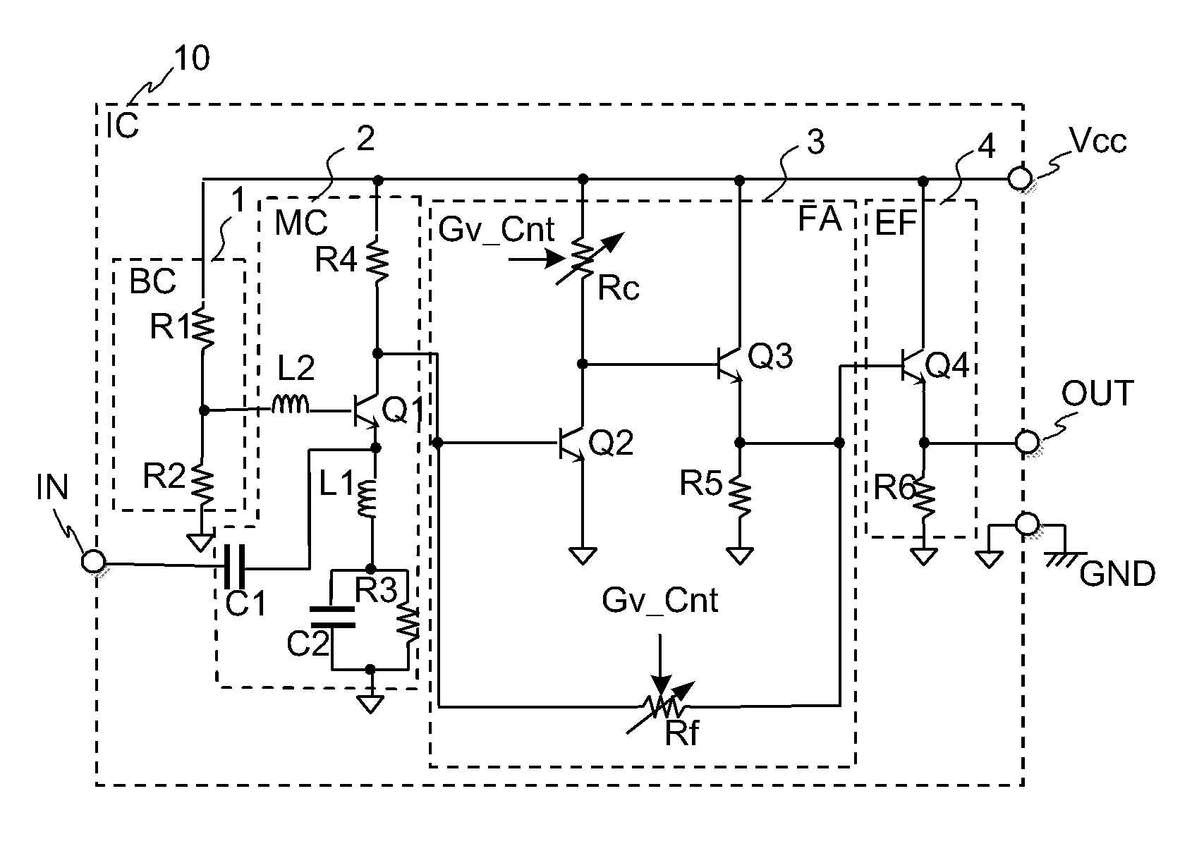
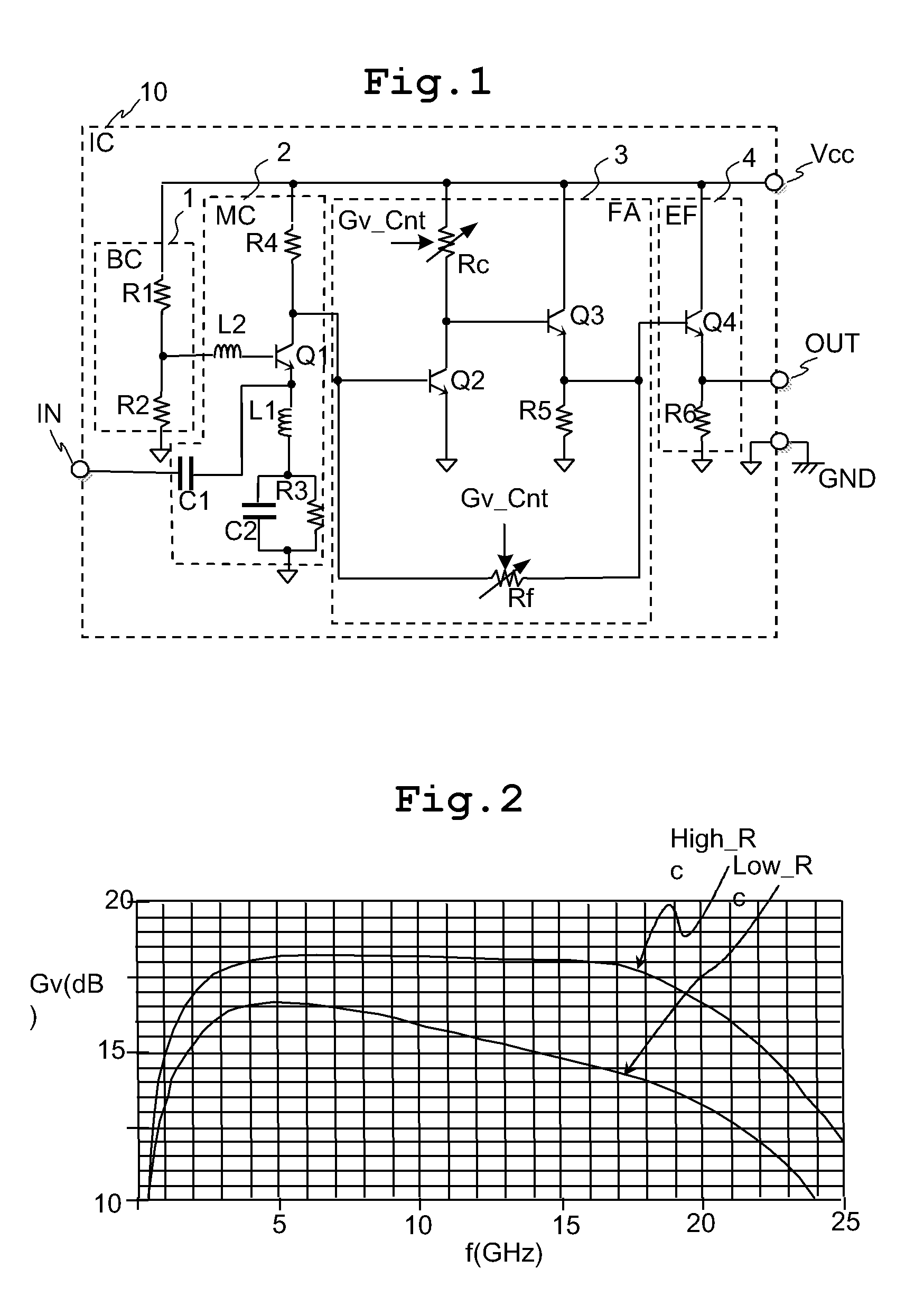
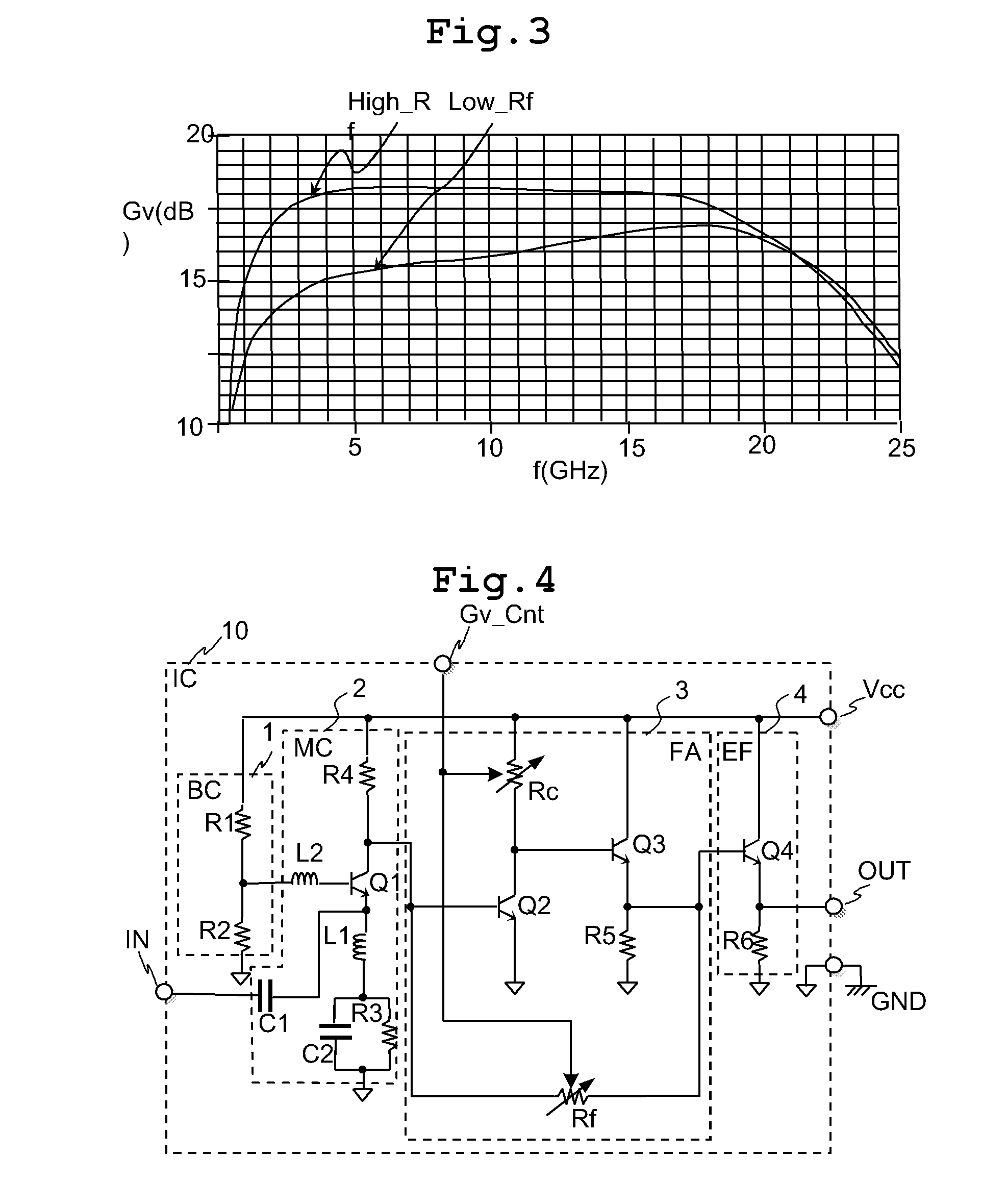
[0054][1] A semiconductor integrated circuit according to a preferred embodiment of the invention has a variable gain resistive feedback amplifier (3) including: a transistor for amplifier (Q2); a load resistance (Rc); a voltage follower for feedback (Q3, R5); and a feedback resistance (Rf).

[0055]A common terminal of an emitter or a source of the transistor for amplifier (Q2) is connected to a predetermined reference voltage (GND).

[0056]An input signal is supplied to an input terminal of the base or gate of the transistor for amplifier (Q2).

[0057]The load resistance (Rc) is connected between an output terminal of the collector or drain ...


PUM


Abstract

The variable gain amplifier includes a bias circuit (BC) 1, a matching circuit (MC) 2, a variable gain resistive feedback amplifier (FA) 3 and an output follower (EA) 4. The resistance values of the load resistance Rc and feedback resistance Rf are changed in cooperation. In a case of making the load resistance Rc a high resistance to set the low noise amplifier to a high gain, the feedback resistance Rf is also made a high resistance, the feedback time constant τfb(c1)≈2π·RfCbe/(1+gmRc) of the closed loop of the resistive negative feedback amplifier 3 becomes substantially constant, and then the amplifier has a gain small in frequency dependency over a wide bandwidth. In a case of making the load resistance Rc a low resistance to set the low noise amplifier to a low gain, the feedback resistance Rf is also made a low resistance. The feedback resistance Rf with the low resistance increases the negative feedback quantity, and thus the amplifier is set to a low gain. Also, the load resistance Rc is made a low resistance, and the feedback time constant τfb(c1) becomes substantially constant. The gain is not lowered further in a high frequency region.

Description

CLAIM OF PRIORITY[0001]The present application claims priority from Japanese application JP 2007-271119 filed on Oct. 18, 2006, the content of which is hereby incorporated by reference into this application.FIELD OF THE INVENTION[0002]The invention relates to a semiconductor integrated circuit having therein a variable gain amplifier, which is mounted in a transceiver for wireless communication or wire communication. Particularly, it relates to a technique useful to offer a variable gain amplifier having a small gain dependent on the frequency over a wide bandwidth.BACKGROUND OF THE INVENTION[0003]In a receiver section of wireless or wire communication system, a low noise amplifier makes a first circuit block which has a gain first, and therefore the noise figure (NF) of the low noise amplifier is added into the noise figure of the system as it is. In the receiver section, the conjugate matching of the antenna and low noise amplifier is performed in order to attain a signal power as...

Claims


Application Information

Patent Timeline
Patent Type & Authority Applications(United States)
IPC IPC(8): H03F3/68
CPCH03F1/342H03F3/195H03F3/50H03F2200/135H03G1/0023H03F2200/294H03F2200/451H03F2203/5036H03F2200/18
Inventor SHIRAMIZU, NOBUHIROMASUDA, TORU
Owner RENESAS ELECTRONICS CORP
Why Eureka
Try Eureka