
Metal-insulator-metal (MIM) switching devices

a switching device and metal-insulator technology, applied in circuit-breaking switches, pulse techniques, instruments, etc., can solve the problems of increasing exponentially, affecting the operation efficiency of the switch, etc., to achieve excellent on-state conductance, wide operating temperature range, and radiation hardness

Active Publication Date: 2009-05-21
RGT UNIV OF CALIFORNIA
View PDF7 Cites 29 Cited by
  • Summary
  • Abstract
  • Description
  • Claims
  • Application Information

AI Technical Summary

Benefits of technology

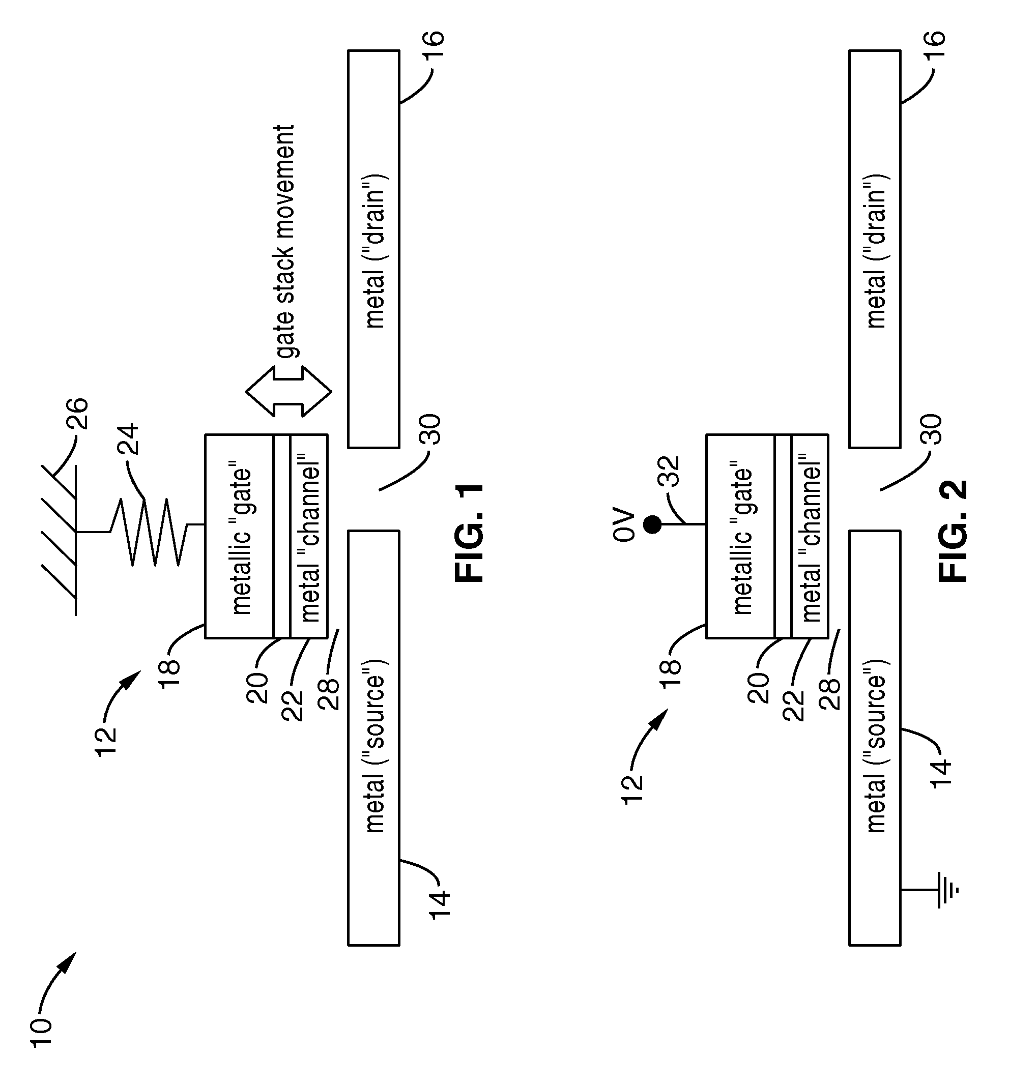
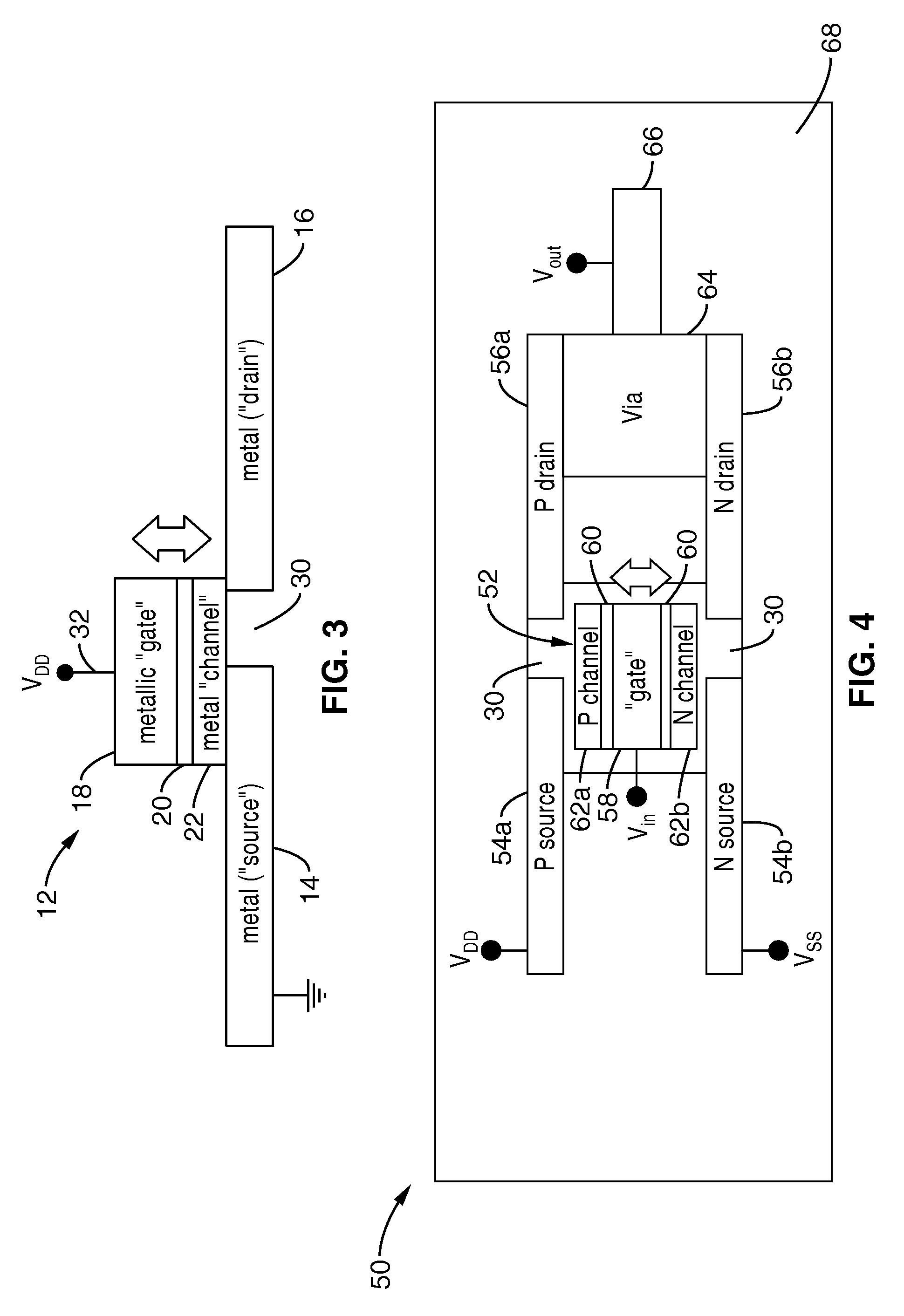
[0017]In one preferred implementation of the above, the means for biasing comprises a cantilever beam coupled between a non-movable anchor and the first gate stack. To simplify construction, the cantilever beam preferably forms the gate electrode of the gate stack, or stacks. To increase maximum operating speed, the volumetric region surrounding the gate stack(s) is preferably fully evacuated, partially evacuated, or filled with a low-pressure substantially non-reactive gas. In a preferred implementation, the channel layer(s) and the pair(s) of output electrodes comprise identical material, or alternatively, materials having approximately equal work functions. Contact is established between the first channel layer and the pair of output electrodes, with a larger portion of the first channel layer in contact with the source electrode than is in contact with the drain electrode. More preferably the contact ratio is on the order of at least twice as much of the channel layer making contact with the source electrode as makes contact with the drain electrode.
[0047]Another aspect of the invention is to provide a NEM switching device wherein said source and drain electrodes are sufficiently separated to prevent leakage current.

Problems solved by technology

Power consumption has emerged as a major challenge for continued scaling of CMOS technology.
In particular, static (leakage) power is an issue because it increases exponentially with reductions in gate length and gate-dielectric thickness.
Dynamic power is difficult to reduce by scaling the supply voltage (VDD), because of threshold voltage (VT) variability and non-scalability due to fundamental thermal limits which dictate that leakage current increases exponentially with decreasing VT.
In general, there exist four main areas to this scaling problem: (1) drain leakage which doubles with each successively smaller generation of CMOS; (2) attempts to ameliorate gate leakage necessitate utilizing advanced gate dielectric materials from which cost and process integration issues arise; (3) threshold voltage control and reduction issues arise with variability resulting in yield issues, and in which non-scalability arises in response to the thermal limit (kT / q) making supply-voltage (VDD) scaling difficult; (4) performance gains as technology scales down are controverted by parasitic resistance and capacitance which seriously limit performance in nanoscale transistors.
However, drain leakage due to quantum-mechanical tunneling and VT variability and non-scalability remain as issues for these approaches in the sub-10 nm gate-length regime.
In addition, the formation of uniform ultra-thin or narrow films and fins present a number of manufacturing challenges.
In addition, the use of high-mobility channel materials poses a myriad of process integration challenges while performance benefits over Si are not dramatic.
Still further, none of these proposed solutions address challenges for radiation hardness and high-temperature operation.

Method used


Image

  • Metal-insulator-metal (MIM) switching devices
  • Metal-insulator-metal (MIM) switching devices
  • Metal-insulator-metal (MIM) switching devices

Examples


embodiment 210

[0136]FIG. 15 illustrates by way of example, an embodiment 210 of a sleep transistor pair with MIM-based NEM switching devices 212a, 212b. Movable gates 214a, 214b, are shown upon whose underside are channels regions 216a, 216b for bridging source 220a to drain 222a, and at the same time source 220b to drain 222b. Drains 222a, 222b are connected, respectively, to separate outputs 224a, 224b. The base of movable gates 214a, 214b is anchored at anchor regions 218a, 218b. Source 220a is coupled to power supply VDD 72, while source 220b is coupled to ground connection VSS 74. Although not shown in this figure, the exemplified structure comprises metallic cantilevers 214a, 214b and conductive channel regions 216a, 216b between which a gate dielectric is disposed, thus forming a MIM structure.

[0137]NEM Device with Tunable Threshold Voltage.

[0138]NEM devices according to the present invention can be fabricated to provide a tunable threshold voltage. At least one embodiment of a NEM switch ...

embodiment 290

[0143]FIG. 19 illustrates a comparison between CMOS 270 and CMIM 290 embodiments with regard to driving of a large capacitive load. Multiple CMOS inverters 272 are shown coupled in series to drive a large capacitive load 274. The series connection is necessary as each MOSFET device has an on-state resistance on the order of kilo-ohms. However, embodiment 290 depicts a single CMIM device 292 capable of driving the same large capacitive load 274, therein reducing power consumption and layout area.

[0144]Characterization of CMIM Devices.

[0145]The gate delay of a CMIM device can be characterized as:

tdelay=telectrical+tmechanical

[0146]The value of telectrical represents a very small value, as it is approximately two orders of magnitude smaller than that of a CMOS device with the same W / L due to the lower on-state resistance and lower capacitance of the CMIM device. In the following analysis it is assumed that the volume within which the channel, or channels, are traversed by the movable ...


PUM


Abstract

A gated nano-electro-mechanical (NEM) switch employing metal-insulator-metal (MIM) technology and related devices and methods which can facilitate implementation of low-power, radiation-hardened, high-temperature electronic devices and circuits. In one example embodiment a gate electrode is configured as a cantilever beam whose free end is coupled to a MIM stack. The stack moves into bridging contact across a source and drain region when the applied gate voltage generates a sufficient electrostatic force to overcome the mechanical biasing of the cantilever beam. A second set of contacts can be added on the cantilever beam to form a complementary switching structure, or to a separate cantilever beam. The switching can be configured as non-volatile in response to stiction forces. NEM circuits provide a number of advantages within a variety of circuit types, including but not limited to: logic, memory, sleep circuits, pass circuits, and so forth.

Description

CROSS-REFERENCE TO RELATED APPLICATIONS[0001]This application claims priority from, and is a 35 U.S.C. § 111(a) continuation of, co-pending PCT international application serial number PCT / US2007 / 067798, filed on Apr. 30, 2007, incorporated herein by reference in its entirety, which claims priority from U.S. provisional application Ser. No. 60 / 796,806 filed on May 1, 2006, incorporated herein by reference in its entirety.STATEMENT REGARDING FEDERALLY SPONSORED RESEARCH OR DEVELOPMENT[0002]Not ApplicableINCORPORATION-BY-REFERENCE OF MATERIAL SUBMITTED ON A COMPACT DISC[0003]Not ApplicableNOTICE OF MATERIAL SUBJECT TO COPYRIGHT PROTECTION[0004]A portion of the material in this patent document is subject to copyright protection under the copyright laws of the United States and of other countries. The owner of the copyright rights has no objection to the facsimile reproduction by anyone of the patent document or the patent disclosure, as it appears in the United States Patent and Tradema...

Claims


Application Information

Patent Timeline
IPC IPC(8): H01L27/092H03K17/687
CPCB82Y10/00H01H1/0094G11C23/00
Inventor KAM, HEIKING, TSU-JAE
Owner RGT UNIV OF CALIFORNIA
Learn More