Multicolored mask process for making display circuitry

a display circuit and multi-colored technology, applied in the field of multi-colored masking process for making display circuits, can solve the problems of affecting the performance and ability to perform alignment of transistor components, affecting the overlay accuracy achievable using traditional photolithography equipment, and applying multiple layers at extremely high speeds

Inactive Publication Date: 2009-05-21
EASTMAN KODAK CO
View PDF8 Cites 21 Cited by
  • Summary
  • Abstract
  • Description
  • Claims
  • Application Information

AI Technical Summary

Benefits of technology

[0033]The invention provides a method for forming aligned layers without the need for expensive alignment equipment and processes. In particularly, the invention can provide a means for making electronic components for active matrix displays with less expensive alignment equipment and processes. Another advantage of the present invention is that it can provide a robust process for forming active matrix electronic components on flexible substrates.

Problems solved by technology

At the other extreme, conventional printing techniques such as offset lithography, flexography, and gravure printing also apply multiple layers at extremely high speeds, although at substantially lower overlay accuracy.
In spite of the potential advantages of flexible substrates, there are many issues affecting the performance and ability to perform alignments of transistor components across typical substrate widths up to one meter or more.
In particular, for example, the overlay accuracy achievable using traditional photolithography equipment can be seriously impacted by substitution of a flexible plastic substrate for the rigid glass substrates traditionally employed.
Three types of registration errors are common in these fabrication processes: fixed errors, scale errors, and local misalignments.
In addition to fixed errors, scale errors may also be substantial.
Errors in pattern scale are cumulative across the substrate and arise from support dimensional change, thermal expansion, and angular placement errors of the substrate with the patterning device.
Although the motion control system impacts angular placement, pattern scale mismatch is largely driven by the characteristics of the support.
Thermal expansion, expansion from humidity or solvent exposure, shrinkage from high temperature exposure, and stress relaxation (creep) during storage of the support all contribute to pattern scale errors.
Further, local pattern mismatch arising from nonisotropic deformations may also occur, particularly since the conveyance process involves applying tension.
Unfortunately, these technologies ultimately produce a flexible electronics component only with the cost structure of current glass based processing.
It is difficult to imagine significant equipment cost difference or throughput advantage, particularly if the added task of distortion compensation is included.
Most of these methods allow self alignment of one layer to another layer, but do not significantly remove the need for very sophisticated alignment steps between several layers.
There are difficulties with the SAIL process, however.
Second, the SAIL process requires high accuracy etch depth control, which may not be consistent with a low cost process.
Finally, a significant limitation of the SAIL process is that layers produced by the mask cannot be fully independent.
As an example, it is particularly challenging to form openings under continuous layers with this approach, an essential element in a matrix backplane design.
Active matrix displays are particularly challenging for electronic component registration and alignment issues, as displays move toward higher resolution, driving the display toward smaller pixel sizes, often with smaller associated electronics.

Method used


Image

  • Multicolored mask process for making display circuitry
  • Multicolored mask process for making display circuitry
  • Multicolored mask process for making display circuitry

Examples


example 1

Colorscale Mask For Active Matrix Display

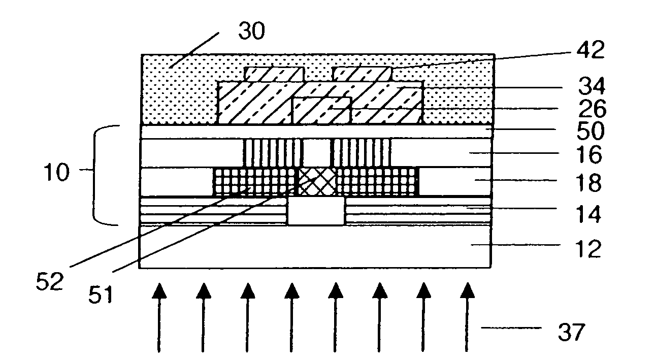
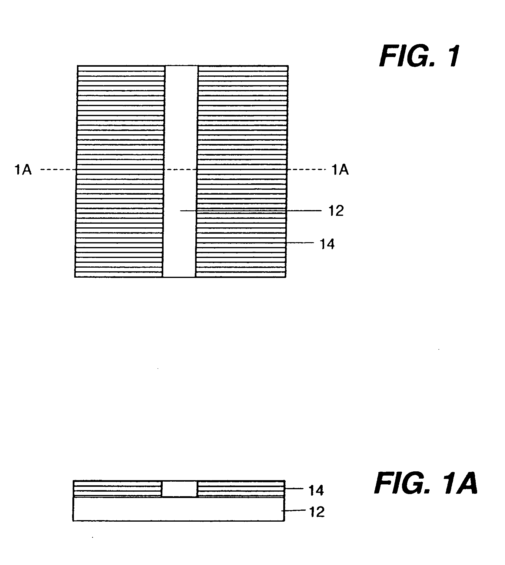
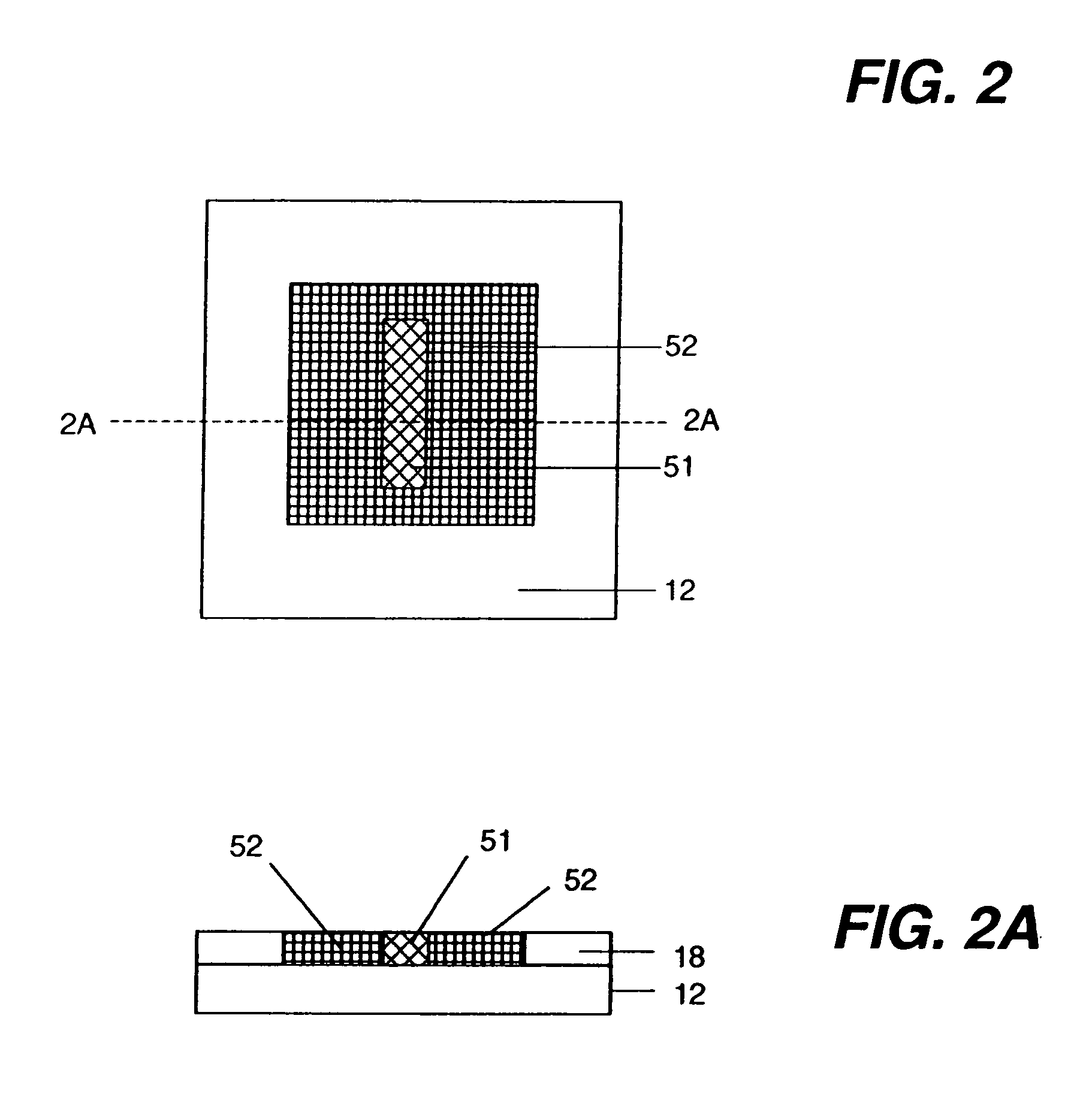
[0224]In this example, an active matrix multicolor mask AM-1 was prepared that contained the patterning information to create an array of pixel circuits for an active matrix display. A schematic diagram of the color absorbing layers for the multicolor mask is shown in FIGS. 17-20. Although the layout shown in FIGS. 17-20 is not drawn exactly to scale, the color-coding of the various components in the active matrix display design is consistent with the previous description. An expanded view of the color patterns in multicolor mask AM-1 for the individual active matrix display pixel circuit is also shown schematically in FIGS. 16A-D. Multicolor mask AM-1 contained red color absorbing layer RCA-1, green color absorbing layer GCA-1, a variable density blue-absorbing layer BCA-1 (an overlay of BCA-1Lo and BCA-1Hi patterns) and planarizing layer P-2. The four patterns in this mask corresponded to separate functional layers of the array of pixel cir...

example 2

Array of Active Matrix Display Pixel Circuits

[0229]In this example, an array of active matrix display pixel circuits was prepared using the multicolor mask AM-1 to pattern transparent electronic materials. The array of pixel circuits were prepared on the same side of the substrate as the multicolor mask.

[0230]The first conductor layer was patterned using a negative etch process and red-sensitive photopatternable material. The sample was coated with 1000 Angstroms of sputtered indium-tin-oxide, which was used as the first conductor layer, applied directly over the planarizing layer P-2. A coating solution was prepared containing 4 g of CF-1 and 0.5 g of the photoinitiator solution CPI-1. The coating solution was spin coated at 2000 RPM for one minute and dried for 2 minutes at 90° C. A 10% PVA coating was applied at 1000 RPM for 2 minutes and dried at 90° C. for 2 minutes. The coating was exposed using red light in such fashion that exposing light passed through the glass support and...

example 3

Array of Active Matrix Display Pixel Circuits on Flexible Support

[0235]In this example, an array of active matrix display pixel circuits was prepared using a multicolor mask AM-2 to pattern transparent electronic materials on a 100 um thick flexible (PEN) support. The display pixel circuits were prepared on the opposite side of the substrate as the color mask. The color absorbing layers in AM-2 had essentially the same layout as for multicolor mask AM-1. A schematic diagram of the color absorbing layers for the multicolor mask is shown in FIGS. 17-20. Although the layout shown in FIGS. 17-20 is not drawn exactly to scale, the color-coding of the various components in the active matrix display design is consistent with the previous description. An expanded view of the color patterns in multicolor mask AM-1 for the individual active matrix display pixel circuit is also shown schematically in FIGS. 16A-D.

[0236]The first step in fabricating the array of display pixel circuits was to pre...


PUM

PropertyMeasurementUnit
transparentaaaaaaaaaa
coloraaaaaaaaaa
optical densitiesaaaaaaaaaa

Abstract

A process for forming a pixel circuit is disclosed comprising: (a) providing a transparent support; (b) forming a multicolor mask having at least four different color patterns; (c) forming integrated electronic components of the pixel circuit having at least four layers of patterned functional material comprising a first conductor, a dielectric, a semiconductor, and a second conductor each layer of patterned functional material corresponding to the four different color patterns of the multicolor mask. The functional material is patterned using a photopattern corresponding to each color pattern.

Description

CROSS-REFERENCE TO RELATED APPLICATIONS[0001]Reference is made to commonly assigned U.S. application Ser. No. ______ (Docket 94377), filed concurrently by Irving et al. and entitled, “COLORED MASK COMBINED WITH SELECTIVE AREA DEPOSITION,” U.S. application Ser. No. ______ (Docket No. 94616), filed concurrently by Irving et al. and entitled “PHOTOPATTERNABLE DEPOSTION INHIBITOR CONTAINING SILOXANE,” U.S. application Ser. No. ______ (Docket 94378), filed concurrently by Irving et al. and entitled “MULTICOLOR MASK,” U.S. application Ser. No. ______ (Docket 94615), filed concurrently by Irving et al. and entitled “INTEGRATED COLOR MASK,” U.S. application Ser. No. ______ (Docket 94376), filed concurrently by Irving et al. and entitled, “GRADIENT COLORED MASK,” and U.S. application Ser. No. ______ (Docket 92336A), filed concurrently by Irving et al. and entitled, “COLORED MASK FOR FORMING TRANSPARENT STRUCTURES.” All the above-identified applications incorporated by reference in their enti...

Claims


Application Information

Patent Timeline
Patent Type & Authority Applications(United States)
IPC IPC(8): G03F7/26G03G7/00
CPCH01L27/3244H01L29/66765H01L27/1214H01L27/1288H01L27/1225H01L29/7869Y10T428/24802H01L2227/323G03F1/14G03F7/2022H10K59/12H10K59/1201
Inventor IRVING, LYN M.LEVY, DAVID H.THAI, LAN B.
Owner EASTMAN KODAK CO
Why Eureka
Try Eureka