

Electrode for Organic Transistor, Organic Transistor, and Semiconductor Device
a technology of organic transistors and transistors, applied in the field of transistors, can solve the problems of limited selection of organic semiconductor materials, difficult to use plastic substrates or films as substrates, and deterioration of transistor characteristics such as electric field effect mobility, etc., to achieve excellent adhesion with a semiconductor layer, reduce energy barriers, and expand the range of choice
- Summary
- Abstract
- Description
- Claims
- Application Information
AI Technical Summary
Benefits of technology
Problems solved by technology
Method used
Image

Examples
embodiment mode 1
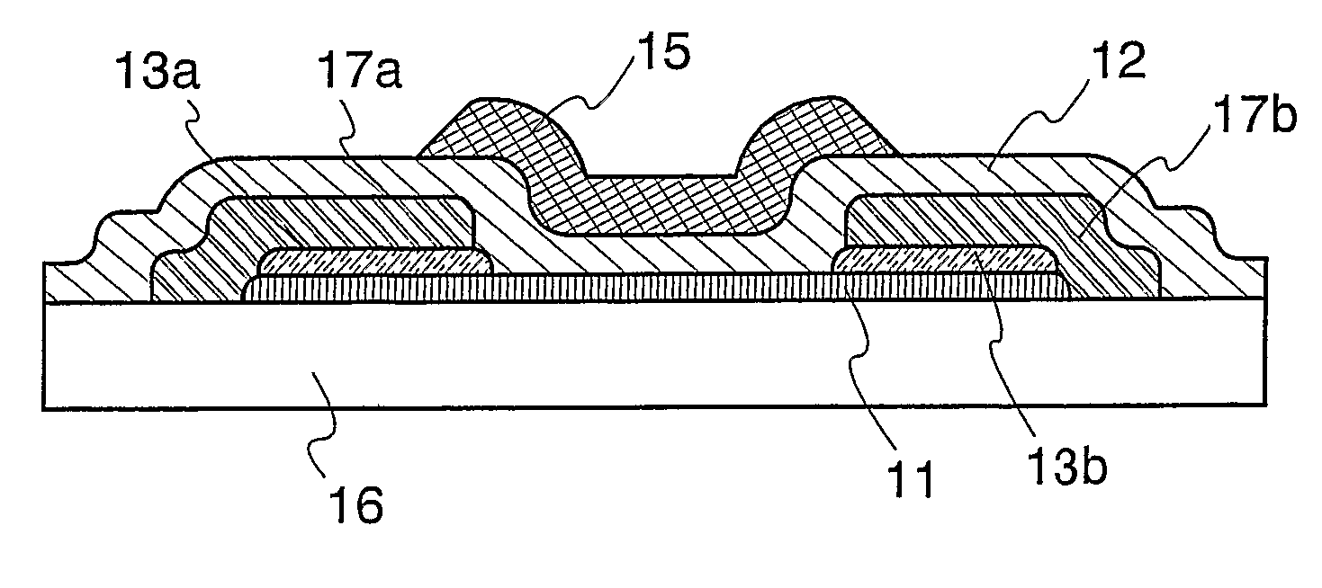
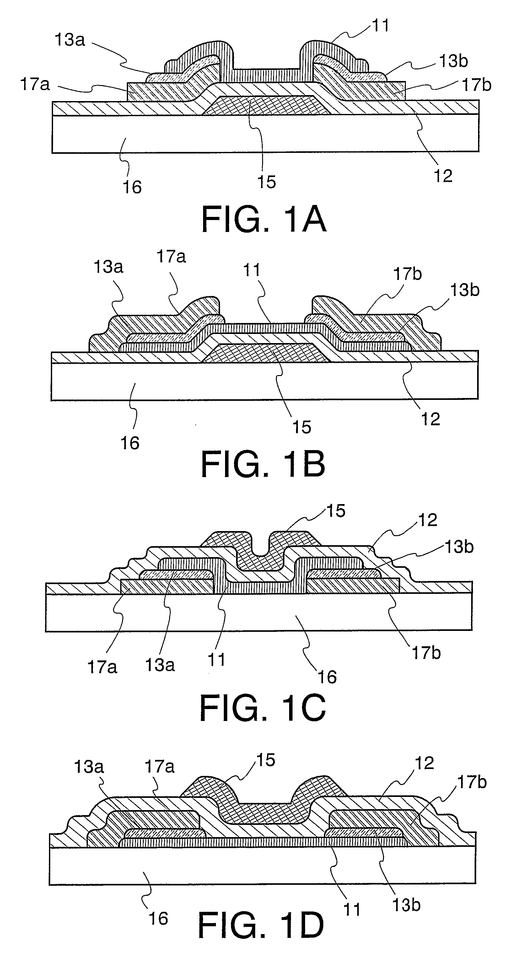
[0084]Structural examples of organic transistors of the present invention are shown in FIGS. 1A to 1D. Note that, in the drawings, reference numeral 11 denotes a semiconductor layer containing an organic semiconductor material; 12, an insulating layer; 15, a gate electrode; and 16, a substrate. The source electrode and the drain electrode include a composite layer 13a and 13b and a conductive layer 17a and 17b formed of a conductive material. An arrangement of each layer or electrode can be appropriately selected in accordance with application of an element.
[0085]A glass substrate; a quartz substrate; an insulating substrate such as a crystalline glass; a ceramic substrate; a stainless steel substrate; a metal substrate (such as tantalum, tungsten, or molybdenum); a semiconductor substrate; a plastic substrate (such as polyimide, acrylic, polyethylene terephthalate, polycarbonate, polyalylate, or polyether sulfone); or the like can be used for the substrate 16. Also, these substrate...
embodiment mode 2
[0107]Subsequently, a structure in which an organic compound used for a composite layer is also used for a semiconductor layer will be described. Since organic compounds that are used for a composite layer and a semiconductor layer are the same in this structure, advantages such as a simple manufacturing process and lower cost are obtained. Moreover, adhesion between a semiconductor layer and a source electrode and a drain electrode, and chemical stability of the interfaces are improved; accordingly, further improvement of transistor characteristics can be expected. Also, improvement in durability of an organic transistor can be expected.
[0108]A semiconductor material which is used in the present invention is not particularly limited; however, the same organic compound as that used for the composite layer described in Embodiment Mode 1 is used.
[0109]A structure of FIG. 1A is used as an example in order to describe the present invention in more detail. As shown in FIG. 1A, a source e...
embodiment mode 3
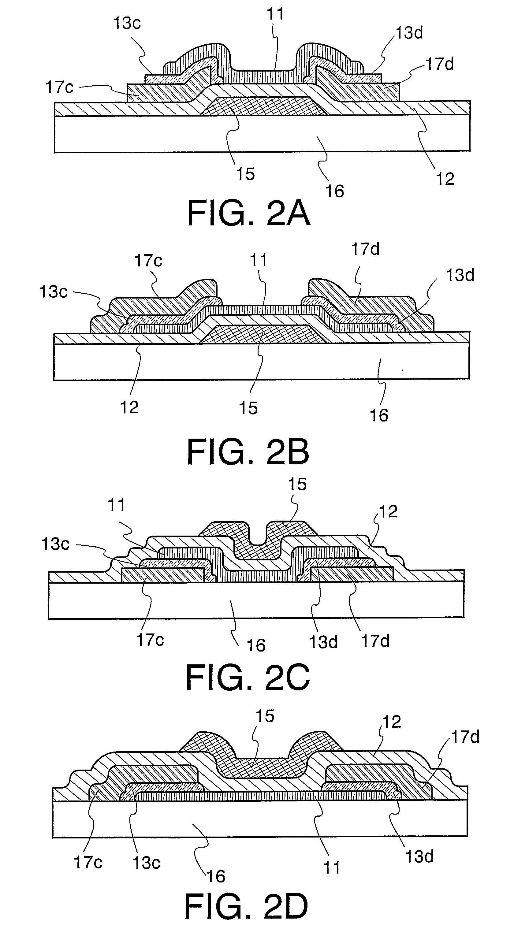
[0112]In this embodiment mode, a structure in which an edge surface of a conductive layers 17a and 17b of an organic transistor are covered with a composite layer and the conductive layers 17a and 17b and the semiconductor layer 11 are not directly in contact with each other will be described with reference to FIGS. 2A to 2D. Structures of FIGS. 2A to 2D are different from Embodiment Mode 1 in that an edge surfaces of conductive layers 17a and 17b or a semiconductor layer 11 of an organic transistor are covered with composite layers. In the structures of FIGS. 2A to 2D, a portion which is not described in this embodiment mode is based on Embodiment Mode 1. Note that FIGS. 2A to 2D correspond to FIGS. 1A to 1D, respectively, and FIGS. 2B and 1B, 2D and 1D are the same.
[0113]As for an organic transistor, depending on an organic material which is used as a semiconductor layer, there is a case where an alignment direction of the organic material highly affects a flow of a current. There...
PUM
 Abstract
Description
Claims
Application Information