Photoelectric conversion device, imaging device and photosensor

a conversion device and imaging device technology, applied in the direction of photometry using electric radiation detectors, optical radiation measurement, instruments, etc., can solve the problems of reducing the aperture ratio and the light collection efficiency, untransmitted light, and poor light utilization efficiency, so as to achieve high photoelectric conversion efficiency and high speed responsivity

Inactive Publication Date: 2009-06-04
FUJIFILM CORP
View PDF11 Cites 15 Cited by
  • Summary
  • Abstract
  • Description
  • Claims
  • Application Information

AI Technical Summary

Benefits of technology

[0011]An object of an illustrative, non-limiting embodiment of the present invention is to provide a photoelectric conversion device, a solid-state im

Problems solved by technology

In this system, since the color filter transmits only light at a limited wavelength, untransmitted light is not utilized and the light utilization efficiency is bad.
Also, in recent years, amid the advance in the fabrication of a multipixel device, the pixel size and in turn, the area of a photodiode part becomes small and this brings about problems of reduction in the aperture ratio and reduction in the light collection efficiency.
However, color separation by the d

Method used


Image

  • Photoelectric conversion device, imaging device and photosensor
  • Photoelectric conversion device, imaging device and photosensor
  • Photoelectric conversion device, imaging device and photosensor

Examples


example 1

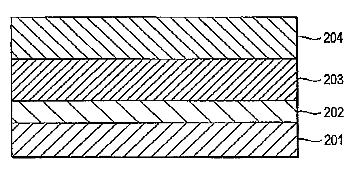
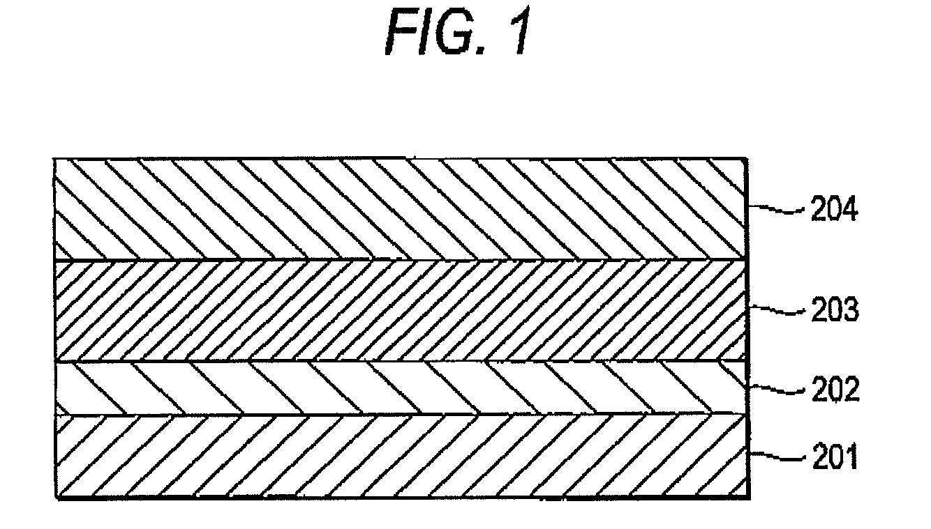
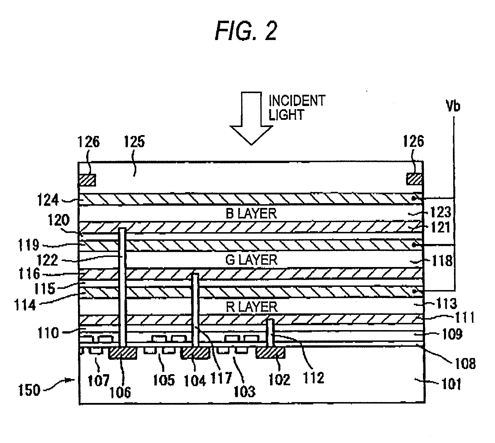
[0198]Amorphous ITO of 100 nm was formed by sputtering on a cleaned glass substrate and patterned by photolithography to produce a pixel electrode while allowing one pixel to be present every each electrode. Thereon, compound A of 100 m and Organic Dye Compound MS-1 of 100 mm and further thereon, silicon oxide of 40 nm each was formed by vacuum heating vapor deposition to produce a photoelectric conversion layer. Furthermore, as the upper electrode, amorphous ITO of 5 nm was formed by sputtering to produce a transparent electrode, whereby a solid-state imaging device was produced (Device 1).

example 2

[0199]A solid-state imaging device (Device 2) was produced thoroughly in the same manner except that in Example 1, Organic Dye Compound (MS-2) of the present invention was used in place of Organic Dye Compound (MS-1) of the present invention.

example 3

[0205]A cleaned ITO (glass) substrate was placed in a vapor deposition apparatus, Organic Dye Compound (MS-3) was vapor-deposited to a thickness of 200 nm, a patterned mask (a mask giving a light-receiving area of 2 mm×2 mm) was provided on the organic thin layer, and aluminum was vapor-deposited to a thickness of 100 nm, whereby a photoelectric conversion device was produced (device 3).


PUM


Abstract

A photoelectric conversion device is provided and includes a photoelectric conversion layer containing a compound represented by the following formula (1). Formula (1):
In the formula, Z1 represents an atomic group for forming a 5- or 6-membered nitrogen-containing heterocyclic ring; Za represents an atomic group for forming a 5- or 6 membered ring; R1 represents a hydrogen atom, an alkyl group, an alkenyl group, an aryl group or a heterocyclic group; L11 to L14 each represents a methine group which may have a substituent or may form a ring with another methine group; p1 represents 0 or 1; n1 represents an integer of 0 to 4 and when n1 is an integer of 2 or more, each L13 or L14 may be the same as or different from every other L13 or L14; M1 represents an ion for neutralizing the electric charge; and m1 represents a number necessary for neutralization of the electric charge; provided that a compound where Z1 is an atomic group forming a thiazoline nucleus or a thiazole nucleus is excluded.

Description

[0001]This application is based on and claims priority under 35 U.S.C. §119 from Japanese Patent Application No. 2007-311167 filed Nov. 30, 2007, the entire disclosure of which is herein incorporated by reference.BACKGROUND OF THE INVENTION[0002]1. Field of the Invention[0003]The present invention relates to a photoelectric conversion device, an imaging device and a photosensor.[0004]2. Description of Related Art[0005]Visible light sensors in the related art are generally a device produced by forming a photoelectric conversion site through, for example, formation of PN junction in a semiconductor such as Si. As for a solid-state imaging device, there is widely used a flat light-receiving device where photoelectric conversion sites are two-dimensionally arrayed in a semiconductor to form pixels and a signal generated in each pixel through photoelectric conversion is charge-transferred and read out according to a CCD or CMOS format. The method for realizing a color solid-state imaging...

Claims


Application Information

Patent Timeline
IPC IPC(8): G01J1/44
CPCG01J1/42H01L27/14609H01L27/14618H01L27/14647H01L27/14692Y02E10/549H01L51/0059H01L51/0064H01L51/4206H01L51/424H01L2251/308H01L27/307H01L2924/0002H10K39/32H10K85/631H10K85/652H10K30/451H10K30/20H10K2102/103H10K30/30H01L2924/00
Inventor SHEN, RUINOMURA, KIMIATSUSUZUKI, HIDEYUKI
Owner FUJIFILM CORP
Why Eureka
Try Eureka