

Plating method
a plating method and technology of a plate are applied in the field of improved plating methods, which can solve the problems of reducing the service life of the plate, so as to reduce the number of nodules, prevent or reduce the effect of circuit defects
- Summary
- Abstract
- Description
- Claims
- Application Information
AI Technical Summary
Benefits of technology
Problems solved by technology
Method used
Image

Examples
example 1
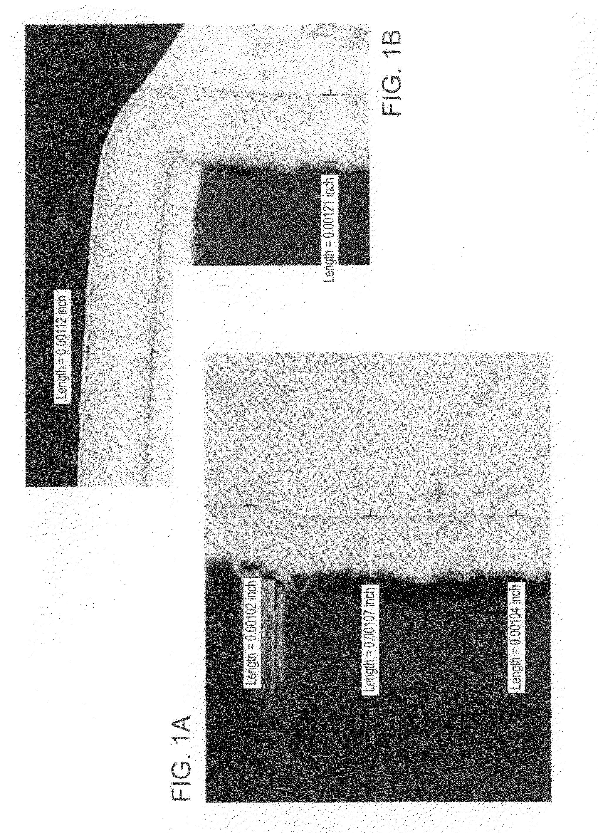
Throwing Power
[0067]A multi-layer copper clad printed circuit board with an array of 0.03 cm, 0.07 cm and 0.09 cm through-holes was pre-cleaned by immersing the board in an aqueous alkaline solution of an organic epoxy solvent of Circuposit™ Conditioner 3302 (obtainable from Rohm and Haas electronic Materials, Marlboro, Mass.) at 70° C. mean temperature for 10 minutes and then rinsed with water.
[0068]The through-hole walls were then desmeared with a permanganate solution of MLB Promoter™ 3308 at a mean temperature of 70° C. for 10 minutes and then rinsed with water. The residues were then neutralized and charge modification was done using a single treatment solution composed of hydroxylammonium acetate (50 g / L), methane sulfonic acid (140 g / L), surfactants (5 g / L), polyelectrolyte (10 g / L) and one liter of water for 5 minutes at 50° C. The board was then rinsed with water.
[0069]A conductive particle coating was then applied to the board. The conductive particle coating was a basic c...
example 2
Comparative
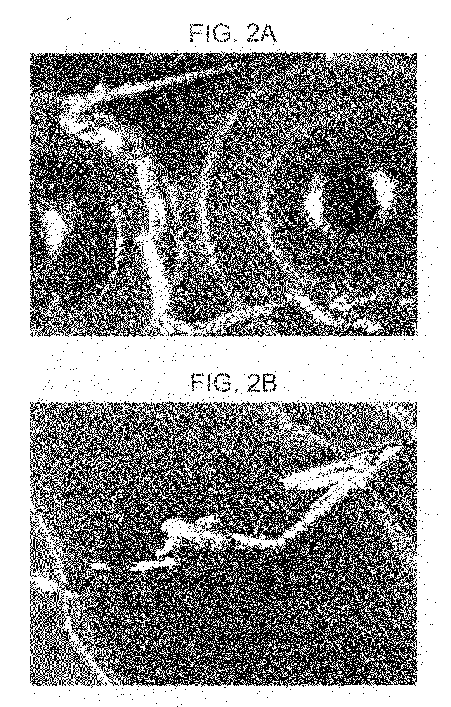
Dendrite Reduction
[0074]Two multi-layer copper clad printed circuit boards with an array of 0.03 cm, 0.07 cm, and 0.09 cm through-holes were pre-cleaned and condition coated by the same method as described in Example 1. After the pre-treatment process was completed each board was placed into an copper electrolyte for copper metal deposition.
[0075]The copper electrolyte included 20 g / L of copper sulfate pentahydrate, 250 g / L of sulfuric acid, 100 ppm of chloride ions, 100 ppm of poly(ethylene glycol), and 0.5 ppm of BSDS. The pH of the electrolyte was maintained from 0 to 1 throughout the plating cycle.
[0076]Each board was placed in a separate plating tank. One board acted as a control where it was plated using a conventional plating process while the other was plated using a current interruption method. The current density for each was maintained at 50 mA / cm2 during copper plating. Each multi-layer board was connected to an emf source along with a copper anode as the coun...
example 3
Comparative
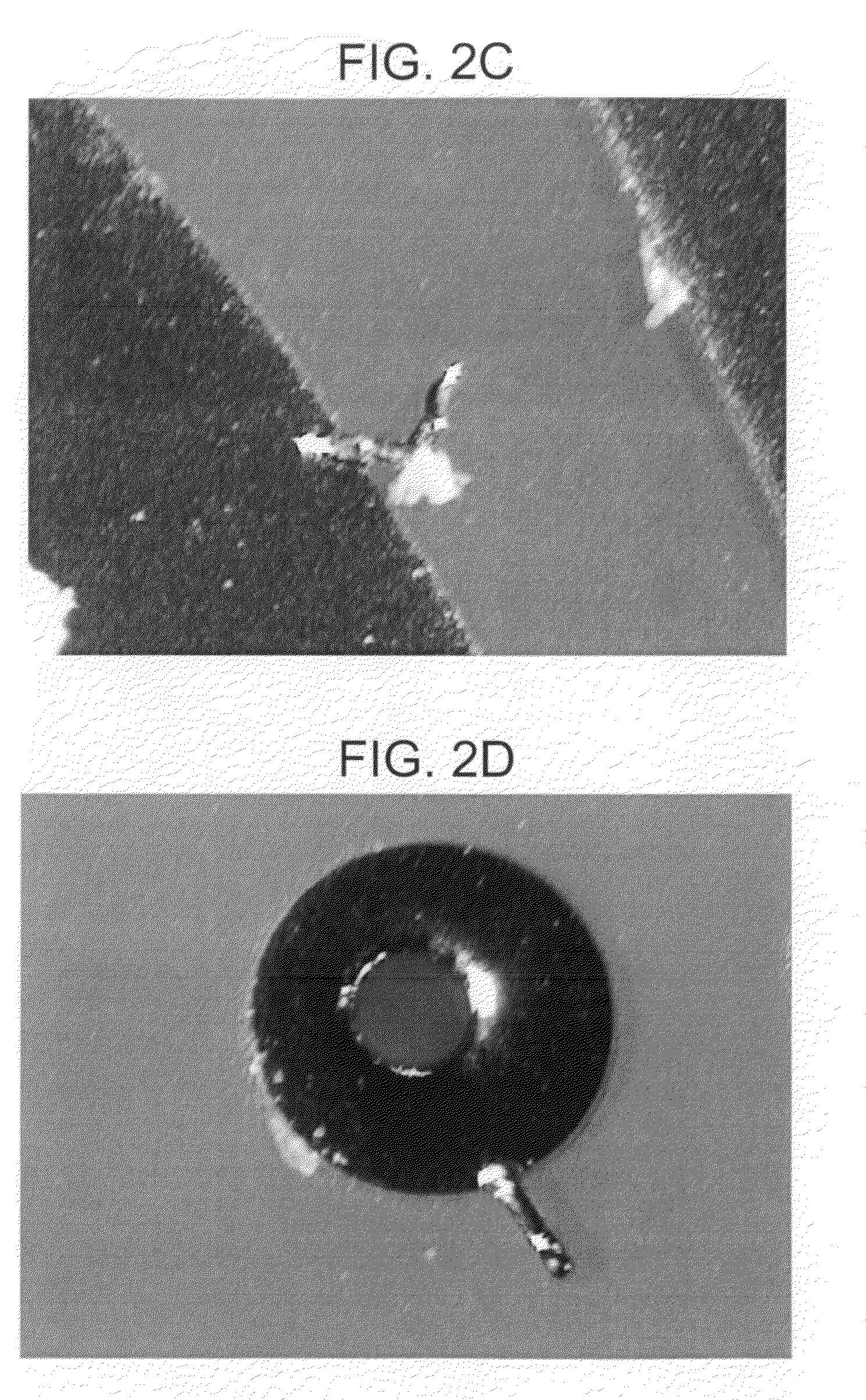
Dendrite Reduction on Double Sided Panels and Throwing Power
[0080]48 FR-4 / epoxy copper clad panels were provided. Holes were drilled in each panel to provide an array of through-holes having diameters of 0.03 cm, 0.07 cm, and 0.09 cm. Each panel was pre-treated to remove accretions from the though-holes using conventional permanganate solutions. Selective portions of the non-conductive parts of each board were conversion coated using a conventional chalcogen solution and conventional processes to make the portions electrically conductive for copper metal deposition.
[0081]Each panel was plated in an aqueous copper electrolyte composed of 50 g / L of copper sulfate pentahydrate, 250 g / L of sulfuric acid, 100 ppm of chloride ions, 300 ppm of poly(ethylene glycol) and 1 ppm of BSDS. The pH of the electrolyte was maintained from 0 to 1 during the plating cycle.
[0082]All of the panels were joined to an emf source along with a copper anode to provide a complete electrical circuit....
PUM
| Property | Measurement | Unit |
|---|---|---|
| diameter | aaaaa | aaaaa |
| current densities | aaaaa | aaaaa |
| current densities | aaaaa | aaaaa |
Abstract
Description
Claims
Application Information