Method for fabricating semiconductor device
- Summary
- Abstract
- Description
- Claims
- Application Information
AI Technical Summary
Benefits of technology
Problems solved by technology
Method used
Image

Examples
first embodiment
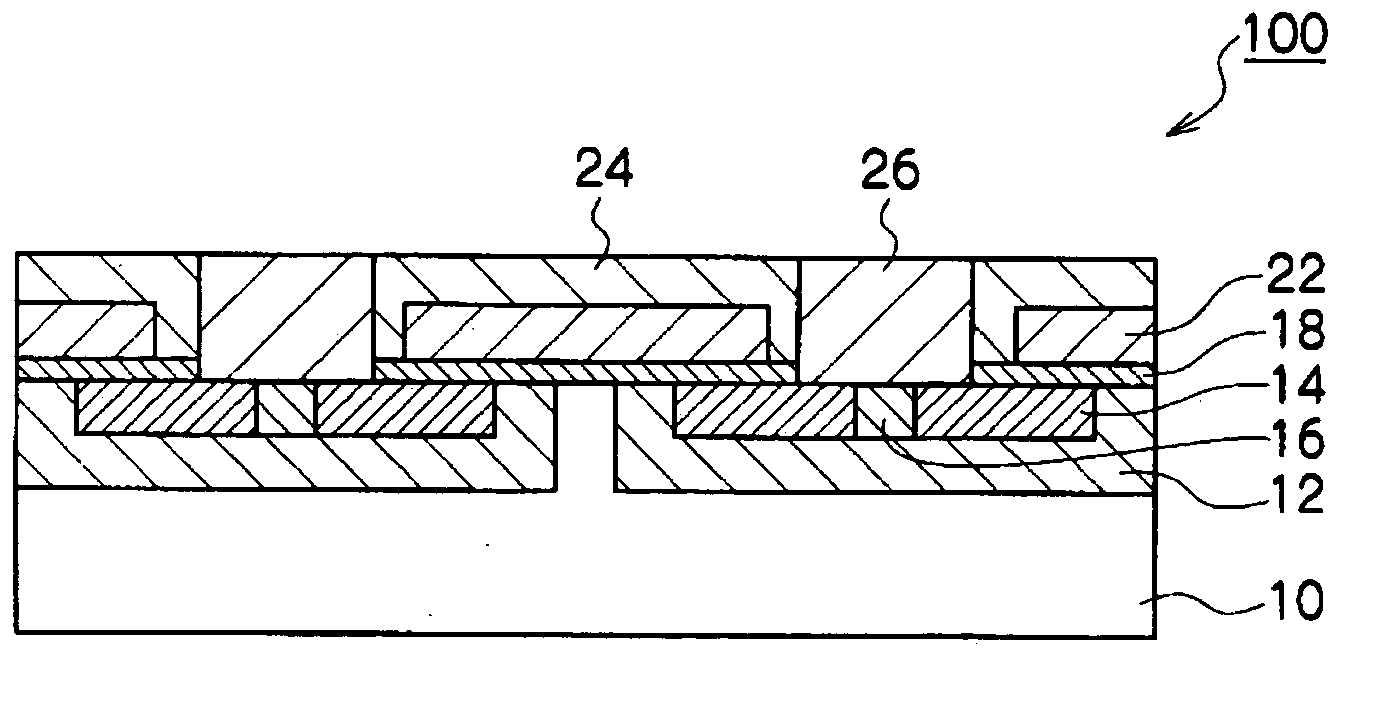
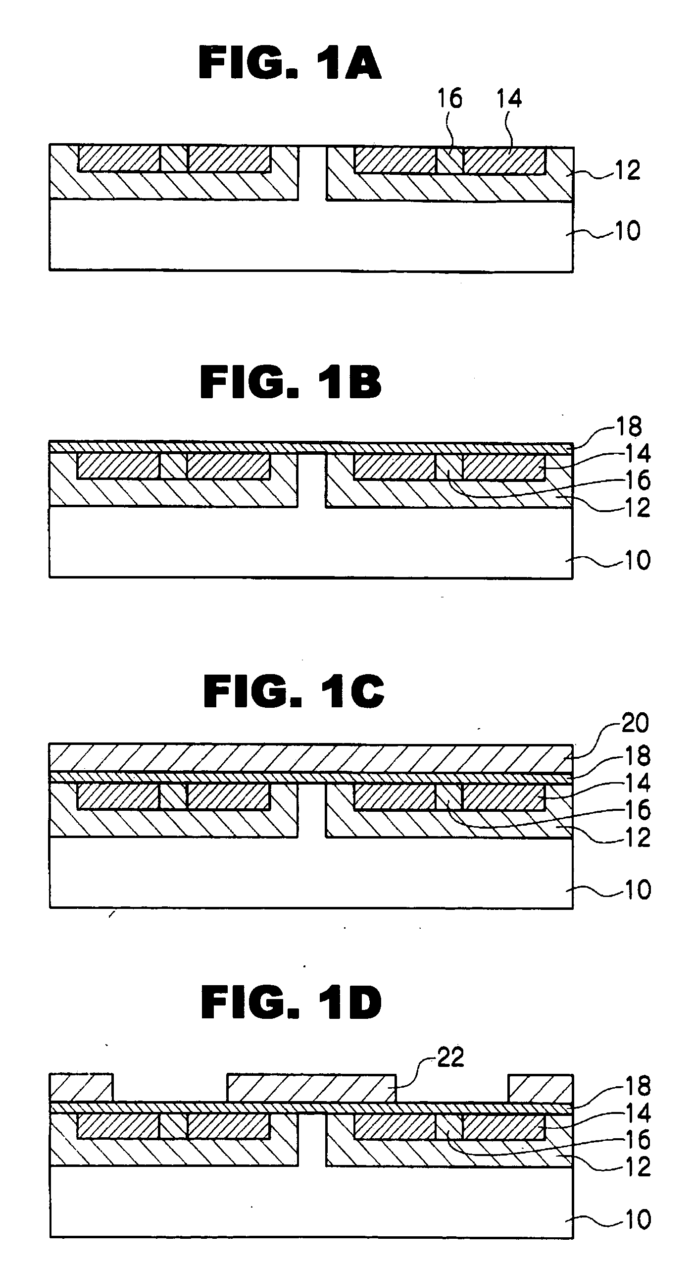
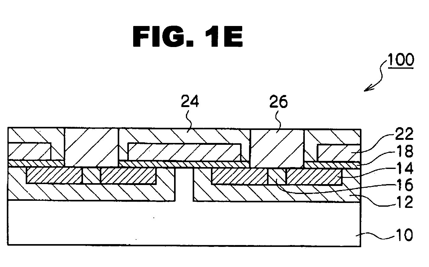
[0030]A method for fabricating a semiconductor device of a first embodiment of the present invention will be described in detail along FIGS. 1A to 1E.
[0031]First, as shown in FIG. 1A, various impurities are injected into a surface layer region of an N-type SiC substrate 10 doped with nitrogen, and a P-type diffusion layer 12, N+ diffusion layer 14, and a P+ diffusion layer 16 are formed. For example, Al ion is injected in the P-type diffusion layer 12 and the P+ diffusion layer 16, and phosphorous is injected in the N+ diffusion layer 14 (a source portion of MOSFET) by, for example, the conventional ion implantation method. Thereafter, the impurities are inactivated, and, at the same time, the crystallinity of the substrate is recovered, for example, for a processing time of several minutes to about 60 minutes at a temperature of about 1500 to 1700° C. in an Ar atmosphere or in a vacuum of not more than 1×10⁻⁵ Pa.
[0032]A gate oxide film 18 is then formed on the surface of the SiC su...
second embodiment
[0046]A method for fabricating a semiconductor device of the second embodiment of the present invention will be described in detail along FIGS. 2A to 2F.
[0047]First, as shown in FIG. 2A, a P-type diffusion layer 32, N+ diffusion layer 34, and P+ diffusion layer 36 are formed in a surface layer region of an SiC substrate 30, as in FIG. 1A.
[0048]Thereafter, as shown in FIG. 2B, an amorphous silicon layer 37 is formed on the SiC substrate 30. The film formation is performed at a temperature of not less than 500° C. and not more than 520° C. in an SiH4 atmosphere or an SiH2Cl2 atmosphere. If the temperature is less than 500° C., the growth speed is slow, whereas the temperature is more than 520° C., polysilicon is formed. The film thickness of the amorphous silicon layer 37 is about ⅓ to ½ of a desired gate oxide film in view of no oxidation of the SiC substrate.
[0049]Next, as shown in FIG. 2C, a gate oxide film 38 is formed by thermal oxidation after the formation of the amorphous sili...
third embodiment
[0054]In a method for fabricating a semiconductor device according to a third embodiment of the present invention, the gate oxide film is directly formed on an SiC substrate by the CVD method, instead of the thermal oxidation of the amorphous silicon layer in the method for fabricating a semiconductor device in the second embodiment.
[0055]Specifically, for example, the gate oxide film is formed, under low pressure, at a temperature of not less than 600° C. and not more than 900° C. in a mixed gas atmosphere of tetra ethyl ortho silicate (TEOS) and oxygen.
[0056]As the mixed gas, SiH4 or Si2H6 may be used instead of TEOS. Further, N2O, NO2, or H2O may be used instead of oxygen.
[0057]If the temperature in the film formation is not less than 900° C., it is not preferable because the carbon atoms in the SiC substrate excessively segregate. Meanwhile, if the temperature is not more than 600° C., it is not preferable because the decomposition of an Si raw material does not progress.
[0058]A...
PUM
 Abstract
Description
Claims
Application Information
 - Generate Ideas
- Intellectual Property
- Life Sciences
- Materials
- Tech Scout
- Unparalleled Data Quality
- Higher Quality Content
- 60% Fewer Hallucinations
Browse by: Latest US Patents, China's latest patents, Technical Efficacy Thesaurus, Application Domain, Technology Topic, Popular Technical Reports.
© 2025 PatSnap. All rights reserved.Legal|Privacy policy|Modern Slavery Act Transparency Statement|Sitemap|About US| Contact US: help@patsnap.com