Large area thin film capacitors on metal foils and methods of manufacturing same

a technology of metal foil and large-area thin film capacitor, which is applied in the direction of thin/thick film capacitor, variable capacitor, fixed capacitor, etc., can solve the problems of microprocessor voltage drop or power droop, power overshoot,

Inactive Publication Date: 2009-09-24
CDA PROCESSING LIABILITY
View PDF9 Cites 24 Cited by
  • Summary
  • Abstract
  • Description
  • Claims
  • Application Information

AI Technical Summary

Problems solved by technology

Noise in the power and ground (return) lines and the need to supply sufficient current to accommodate the faster circuit switching has become an increasingly important problem.
If the response time of the voltage supply is too slow, the microprocessor will experience a voltage drop or power droop that will exceed the allowable ripple voltage and noise margin and the IC will trigger false gates.
Additionally, as the IC powers up, a slow response time will result in power overshoot.
This requires complex electrical routing which leads to inductance.
Embedded capacitors in printed wiring boards made by such techniques, however, are subject to additional requirements other than the capacitance density.
In particular, once the capacitors are embedded they cannot be replaced like surface mounted capacitors.
Achieving 100% embedded capacitor yield is especially troublesome where it is desirable for a large number of embedded capacitors to occupy the area under a semiconductor such as an IC mounted on the printed wiring board.

Method used


Image

  • Large area thin film capacitors on metal foils and methods of manufacturing same
  • Large area thin film capacitors on metal foils and methods of manufacturing same
  • Large area thin film capacitors on metal foils and methods of manufacturing same

Examples


example 1

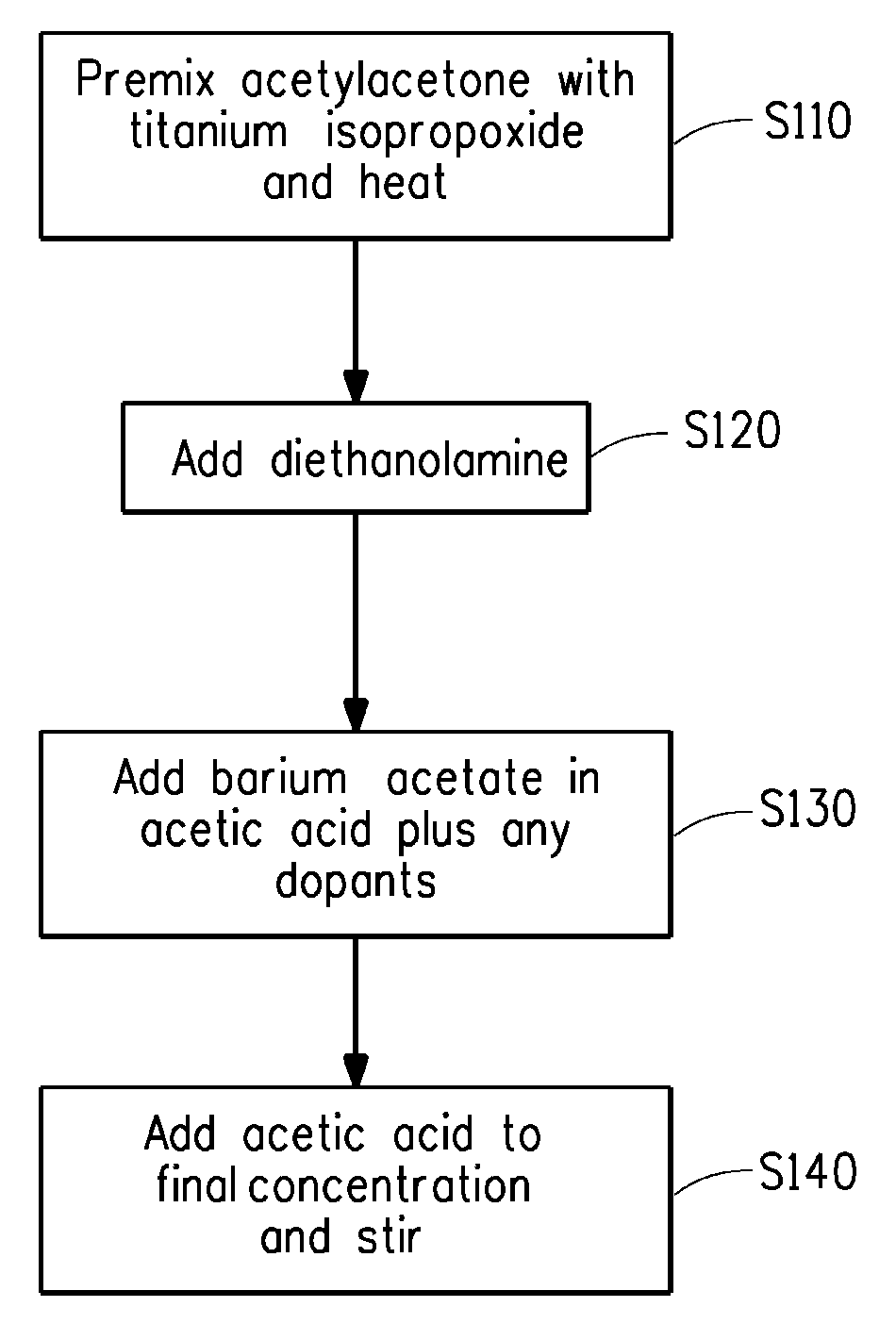
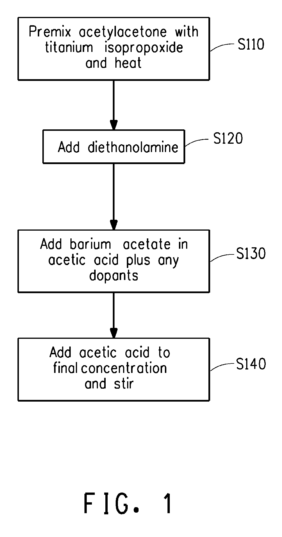
[0058]A 0.38 mol solution of “undoped” or pure barium titanate dielectric precursor solution was prepared according to the method of FIG. 1 from the following:

Barium acetate2.6gTitanium isopropoxide2.9mlAcetylacetone2.0gAcetic acid22.1gDiethanolamine0.3g

The 0.38 mol barium titanate dielectric precursor solution was diluted to 0.3 mole concentration by use of additional acetic acid.

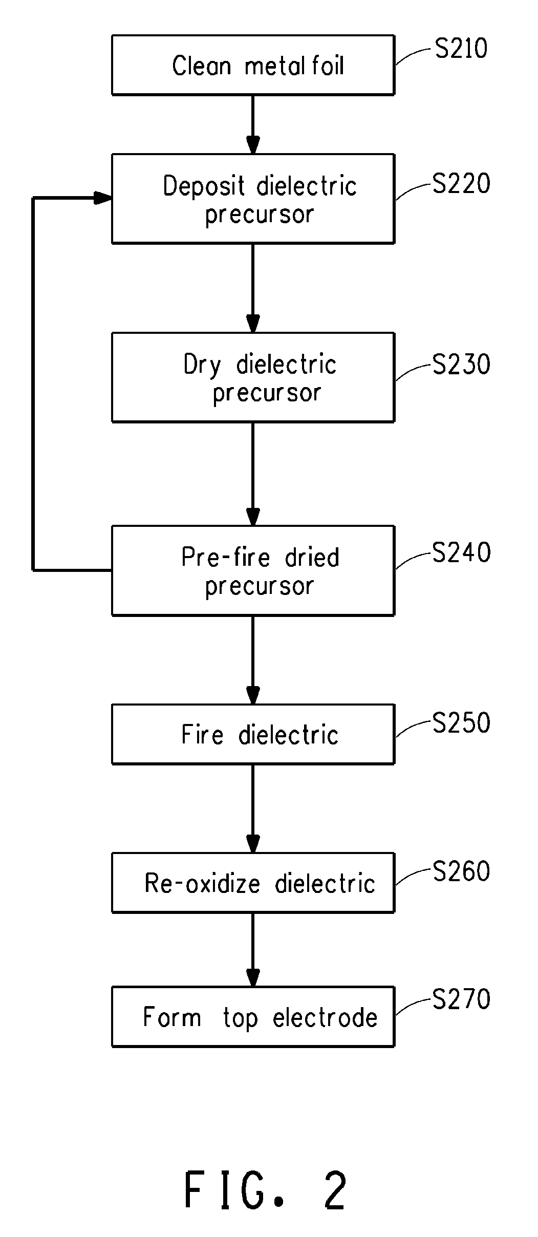
[0059]Capacitor on foil samples were prepared. For each sample, a first layer of the 0.3 mol dielectric precursor solution was deposited on to the drum side of a 2 inch by 2 inch ½ oz (18 micrometers thick) cleaned copper foil (obtained from Oak Mitsui) using spin coating. The coating speed was 3000 rpm. The precursor solution was then dried in air on a hot plate at 250° C. for 7 minutes. The dried thickness was approximately 0.1 micrometers. The process of spin coating deposition and drying was repeated until 6 layers had been deposited.

[0060]The multiple dried dielectric precursor layers on the copper fo...

example 2

[0062]A 0.38 mol barium titanate dielectric precursor solution was prepared as described in Example 1, except that the dielectric precursor solution was doped with 0.07 mole % of manganese by adding 0.001 g of manganese acetate tetrahydrate to the barium acetate solution in the step S130 of the method shown in FIG. 1. The 0.38 mol barium titanate dielectric precursor solution was diluted to a 0.25 mole solution by use of additional acetic acid.

[0063]Several samples were prepared using the process as discussed with regard to FIG. 2. A first layer of the 0.25 mol dielectric precursor solution was deposited using rod coating on to a 5 inch by 5 inch, 25 micrometers thick, nickel foil obtained from All Foils. The precursor solution was then dried on a hot plate at 100° C. for 5 minutes. The dried dielectric precursor was pre-fired at 400° C. for 10 minutes in air. The ramp rate of the hot plate during the heating phase was approximately 10° C. per minute. The process of rod coating depo...

example 3

[0066]A 0.38 mol barium titanate dielectric precursor solution was prepared as described in Example 1, except that the dielectric precursor solution was doped with 0.07 mole % of manganese by adding 0.001 g of manganese acetate tetrahydrate to the barium acetate solution in the step S130 of the method shown in FIG. 1.

[0067]Capacitor on foil samples were prepared. For each sample, a first layer of the doped 0.38 mol barium titanate dielectric precursor solution was deposited by spin coating on to the drum side of a 2 inch by 2 inch ½ oz (18 micrometers thick) cleaned copper foil obtained from Oak Mitsui. The coating speed was 3000 rpm. The precursor solution was then dried in air on a hot plate at 250° C. for 7 minutes. The dried precursor was then prefired for 10 minutes in a moist nitrogen / forming gas mixture that was created by bubbling a mixture of nitrogen and forming gas (99% nitrogen and 1% hydrogen) through a water bath at approximately 20° C. to create a gas atmosphere with ...


PUM

PropertyMeasurementUnit
temperatureaaaaaaaaaa
partial pressureaaaaaaaaaa
temperatureaaaaaaaaaa

Abstract

Disclosed are a method of making a dielectric on a metal foil, and a method of making a large area capacitor that includes a dielectric on a metal foil. A dielectric precursor layer and the base metal foil are prefired at a prefiring temperature in the range of 350 to 650° C. in a moist atmosphere that also comprises a reducing gas. The prefired dielectric precursor layer and base metal foil are subsequently fired at a firing temperature in the range of 700 to 1200° C. in an atmosphere having an oxygen partial pressure of less than about 10−6 atmospheres to produce a dielectric. The area of the capacitor made according to the disclosed method may be greater than 10 mm2, and subdivided to create a multiple individual capacitor units that may be embedded in printed wiring boards. The dielectric is typically comprised of crystalline barium titanate or crystalline barium strontium titanate.

Description

TECHNICAL FIELD[0001]The present invention pertains to capacitors that may be embedded in printed wiring boards, and more particularly to capacitors that include a thin film dielectric formed on a metal foil.RELATED ART[0002]Semiconductor devices including integrated circuits (IC) are operating at increasingly higher frequencies and higher data rates and at lower voltages. Noise in the power and ground (return) lines and the need to supply sufficient current to accommodate the faster circuit switching has become an increasingly important problem. In order to provide low noise and stable power to the IC, low impedance in the power distribution system is required. The higher operating frequencies (higher IC switching speeds) mean that voltage response times to the IC must be faster. Lower operating voltages require that allowable voltage variations (ripple) and noise become smaller. For example, as a microprocessor IC switches and begins an operation, it calls for power to support the...

Claims


Application Information

Patent Timeline
Patent Type & Authority Applications(United States)
IPC IPC(8): B05D5/12H01G7/00H05K3/30
CPCH01G4/1227H01G4/33H05K1/162H05K3/1291Y10T29/43H05K2201/0355H05K2203/1126Y10T29/4913H05K2201/0175
Inventor SUH, SEIGIKIM, ESTHERBORLAND, WILLIAMPALANDUZ, CENGIZ AHMET
Owner CDA PROCESSING LIABILITY
Why Eureka
Try Eureka