Method for manufacturing photoelectric conversion device
Inactive Publication Date: 2009-10-29
SEMICON ENERGY LAB CO LTD
View PDF7 Cites 20 Cited by
Summary
Abstract
Description
Claims
Application Information
AI Technical Summary
This helps you quickly interpret patents by identifying the three key elements:
Problems solved by technology
Method used
Benefits of technology
Benefits of technology
[0011]In the case where a hydrogenion implantation separation method is employed, a single crystal silicon thin film which is homogeneous can be formed at low temperature as compared with the case where a SIMOX method or a method in which thinning is performed utilizing grinding or polishing after bonding is used. Further, a single crystal silicon substrate from which a single crystal silicon thin film has been separated can be reused, so that effective utilization of resources can be achieved.
[0013]However, increase in the acceleration voltage of an ion implantation apparatus has limitation based on the aspect of the apparatus, or radiation rays which are safety hazard might be generated due to increase of the acceleration voltage. Therefore, it is not easy to increase the acceleration voltage in order to obtain a single crystal silicon thin film with a predetermined thickness. Further, in the case of a conventional apparatus, since it is difficult to perform irradiation with a large amount of ions with the acceleration voltage increased, a long period of time is necessary for obtaining a predetermined amount of ions implanted into a single crystal silicon, which results in longer takt time.
[0024]According to an embodiment to be disclosed of the invention, the thickness of the single crystal semiconductor layer is increased by utilizing an epitaxial growth technique. Therefore, it is possible to increase photoelectric conversion efficiency while suppressing the consumption of a raw material. Further, since a surface layer of a single crystal semiconductor substrate is separated as a thin slice to be used as a single crystal semiconductor layer, it is possible to reduce the consumption of a single crystal semiconductor as a raw material. Further, since the thickness of the single crystal semiconductor layer to be required is not large, problems due to an acceleration voltage at the time of ion irradiation can be solved. Further, the single crystal semiconductor substrate from which the single crystal semiconductor layer has been separated can be reused repeatedly.
[0025]Note that according to an embodiment to be disclosed of the invention, after a crystalline semiconductor layer (which may be called a buffer layer) is formed over a single crystal semiconductor layer, a semiconductor layer with low crystallinity (for example, an amorphous semiconductor layer) is formed over the crystalline semiconductor layer. Accordingly, the semiconductor layer can be prevented from being peeled due to heat treatment or the like at the time of epitaxial growth. That is, the single crystal semiconductor layer with enough thickness can be formed with high yield by an epitaxial growth method.
[0026]As described above, by using an embodiment to be disclosed of the invention, the resources can be effectively utilized and a photoelectric conversion device having an excellent photoelectric conversion characteristic can be obtained.
Problems solved by technology
However, increase in the acceleration voltage of an ion implantation apparatus has limitation based on the aspect of the apparatus, or radiation rays which are safety hazard might be generated due to increase of the acceleration voltage.
Further, in the case of a conventional apparatus, since it is difficult to perform irradiation with a large amount of ions with the acceleration voltage increased, a long period of time is necessary for obtaining a predetermined amount of ions implanted into a single crystal silicon, which results in longer takt time.
Method used
Image
Click on the blue label to locate the original text in one second.
Reading with bidirectional positioning of images and text.
Examples
embodiment 1
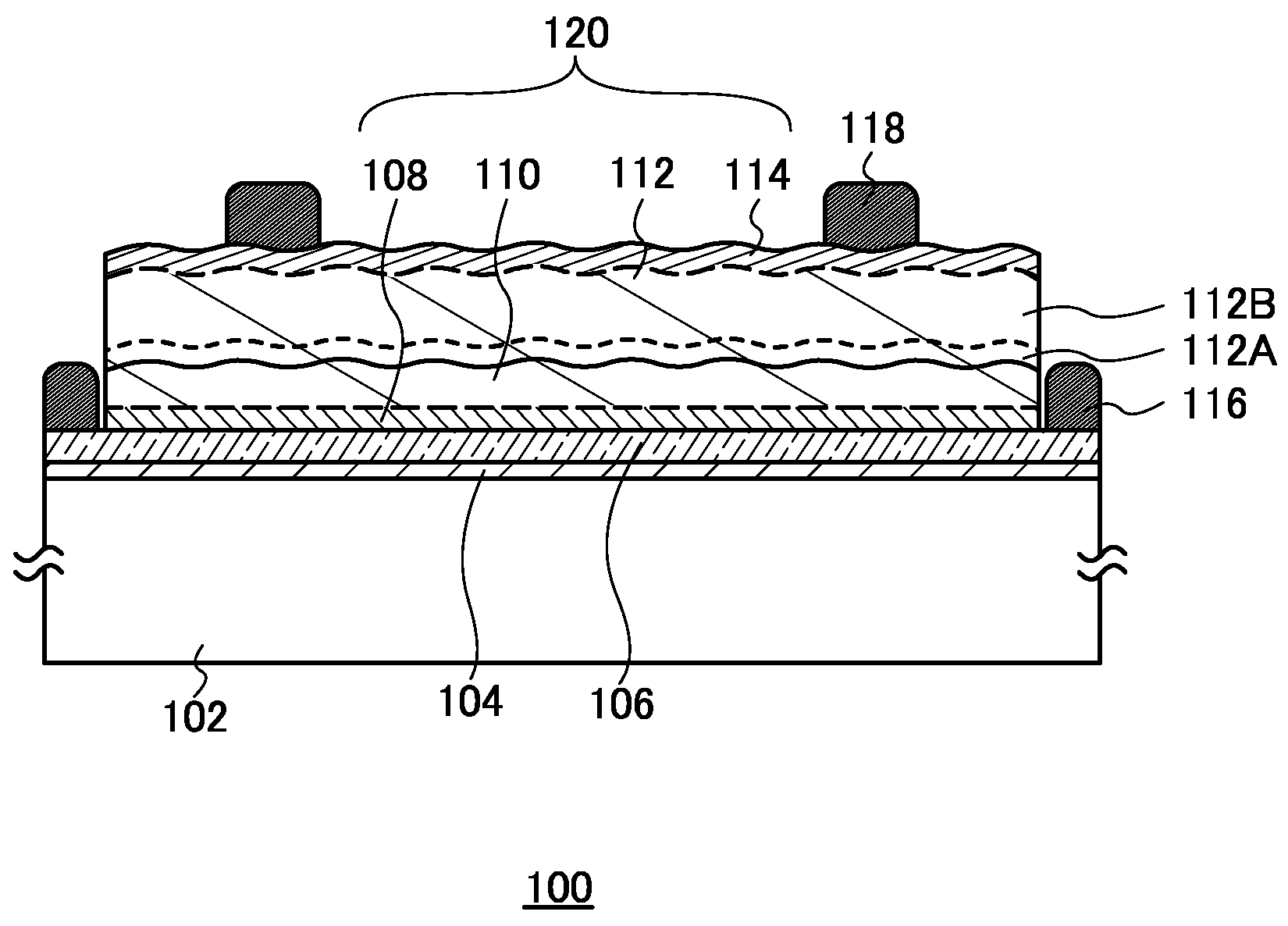
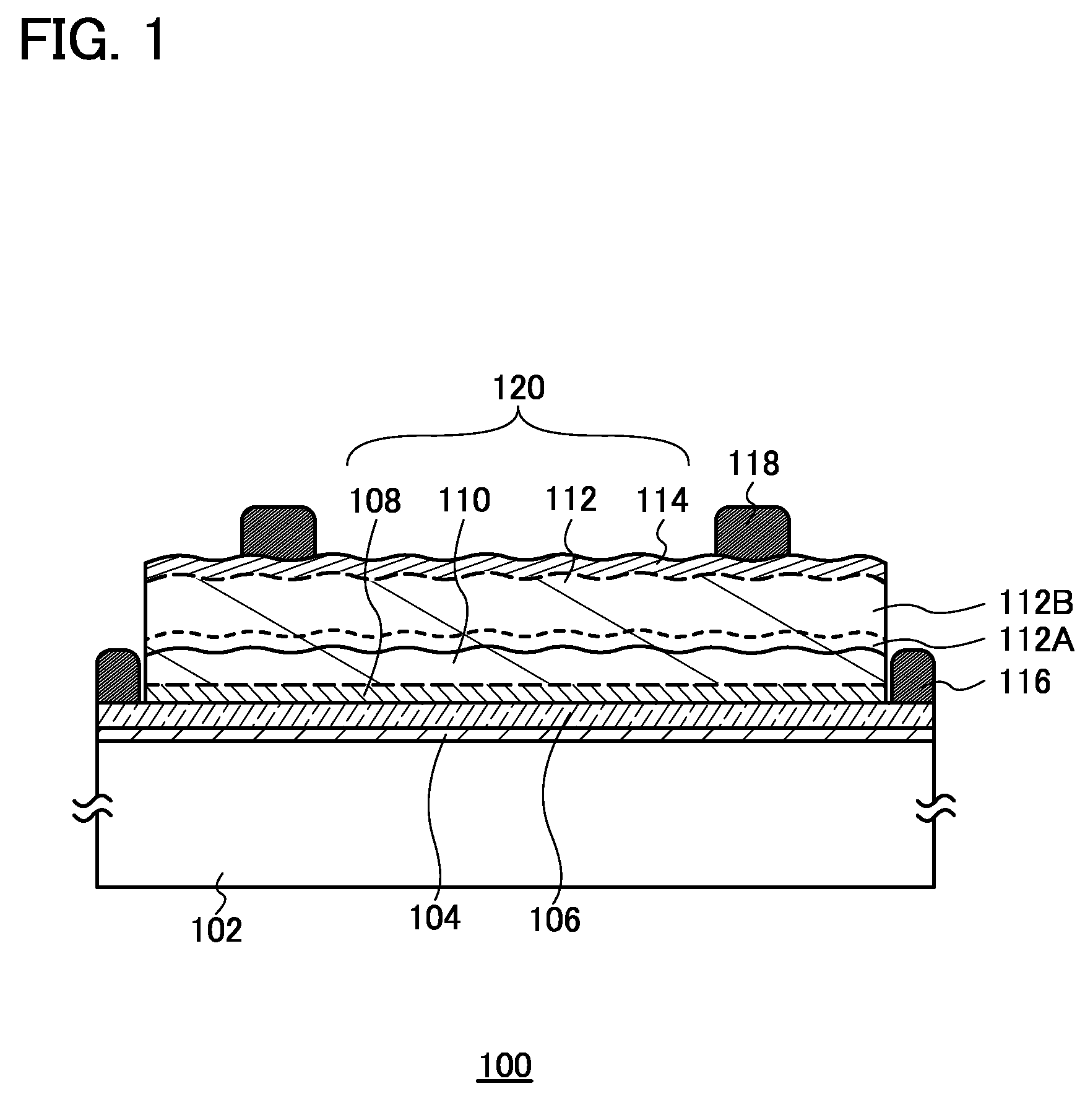
[0054]FIG. 1 illustrates a schematic cross-sectional view of a photoelectric conversion device 100 according to this embodiment. FIG. 2 illustrates a schematic top view (plan view) of the photoelectric conversion device 100 according to this embodiment. Note that FIG. 1 illustrates an example of a cross-sectional view along O-Pin FIG. 2.
[0055]The photoelectric conversion device 100 described in this embodiment has a structure in which an insulating layer 104, a first electrode 106, and a unit cell 120 are stacked in order on a supporting substrate 102. Here, the unit cell 120 has a layered structure of a first impurity semiconductor layer 108 having one conductivity type, a first single crystal semiconductor layer 110, a second single crystal semiconductor layer 112, and a second impurity semiconductor layer 114.
[0056]An auxiliary electrode 116 is formed in an area of the first electrode 106 where the unit cell 120 is not formed, so that electric energy can be extracted. Further, a ...
embodiment 2
[0144]This embodiment describes an example of a method for manufacturing a photoelectric conversion device, which is different from that in the foregoing embodiment. Specifically, although the foregoing embodiment describes, taking (1) as an example, the formation order of the embrittlement layer 105, the first impurity semiconductor layer 108, the first electrode 106, and the insulating layer 104, this embodiment describes examples (2) to (4). Note that a manufacturing process other than the formation order of the embrittlement layer 105, the first impurity semiconductor layer 108, the first electrode 106, and the insulating layer 104 is similar to that of the foregoing embodiment; therefore, the description thereof is omitted.
[0145]The example (2) is described below with reference to FIGS. 10A to 10D.
[0146]First, the protective layer 107 is formed on one surface of the single crystal semiconductor substrate 103. Then, the single crystal semiconductor substrate 103 is irradiated wi...
embodiment 3
[0163]This embodiment describes an example of a method for manufacturing a photoelectric conversion device, which is different from those of the foregoing embodiments.
[0164]FIG. 22 illustrates an example of a photoelectric conversion device which is formed by directly bonding the first electrode 106 and the supporting substrate 102 to each other. In the case where the first electrode 106 has a smooth surface, for example, in the case where the first electrode 106 has a surface with an average surface roughness (Ra) of 0.5 nm or less, preferably 0.3 nm or less, the first electrode 106 and the supporting substrate 102 can be bonded to each other without formation of the insulating layer 104 (see FIG. 1 and the like).
[0165]The bonding is performed by attaching the surface of the first electrode 106 and the surface of the supporting substrate 102 which are sufficiently cleaned to each other. It is needless to say that before the bonding, the surface of the first electrode 106 and / or the...
PUM
Abstract
An embrittlement layer is formed in the single crystalsemiconductor substrate and a first impuritysemiconductor layer, a first electrode, and an insulating layer are formed on one surface of the single crystalsemiconductor substrate. After attaching the insulating layer and a supporting substrate to each other to bond the single crystal semiconductor substrate and the supporting substrate, the single crystal semiconductor substrate is separated along the embrittlement layer to form a stack including a first single crystal semiconductor layer. A first semiconductor layer and a second semiconductor layer are formed over the first single crystal semiconductor layer. A second single crystal semiconductor layer is formed by solid phase growth. A second impurity semiconductor layer having a conductivity type opposite to that of the first impurity semiconductor layer is formed on the second single crystal semiconductor layer. A second electrode is formed on the second impurity semiconductor layer.
Application Information
Patent Timeline
Application Date:The date an application was filed.
Publication Date:The date a patent or application was officially published.
First Publication Date:The earliest publication date of a patent with the same application number.
Issue Date:Publication date of the patent grant document.
PCT Entry Date:The Entry date of PCT National Phase.
Estimated Expiry Date:The statutory expiry date of a patent right according to the Patent Law, and it is the longest term of protection that the patent right can achieve without the termination of the patent right due to other reasons(Term extension factor has been taken into account ).
Invalid Date:Actual expiry date is based on effective date or publication date of legal transaction data of invalid patent.

