System and method for the manufacture of semiconductor devices by the implantation of carbon clusters

a technology of carbon clusters and silicon chips, which is applied in the direction of semiconductor devices, irradiation devices, electric discharge tubes, etc., can solve the problems of increasing the leakage current of usj transistors, difficult formation of usjs, and high cost of gesup>+/sup> implants, so as to improve the mobility of nmos transistors, improve the accuracy and control of equipment, and increase the carrier mobility

Inactive Publication Date: 2009-11-19
SEMEQUIP
View PDF22 Cites 21 Cited by
  • Summary
  • Abstract
  • Description
  • Claims
  • Application Information

AI Technical Summary

Benefits of technology

[0019]There is a secondary benefit to the process in accordance with the present invention that is of great economic value; namely, amorphization of the silicon by the carbon cluster implant and the subsequent boron cluster implant. In particular, it is known in the art that implantation of large boron clusters amorphize the crystalline silicon lattice, resulting in a large reduction in ion channeling. Channeling is known to significantly increase the junction depth of a dopant implant thereby making USJ formation difficult. Channeling is typically controlled by first conducting a damage implant, for example by Ge+ atoms, to amorphise the silicon prior to forming the PMOS source / drain extensions by implanting boron. The Ge+ implant is expensive to perform, and has also been shown to create defects at its end-of-range which increases leakage currents in the USJ transistors, in certain cases by several orders of magnitude. Thus, replacing the conventional boron implant by a boron cluster, such as B18HX+, obviates the need for the Ge implant in many cases, and does not generate the defect structures associated with leakage. This is of great economic value since is removes a costly implant from the process flow, increases yield, and reduces leakage current in the integrated circuits. Unfortunately, the boron cluster implant can never entirely eliminate channeling, since before the critical dose for amorphization is reached, a fraction of the boron cluster implant has been performed, and has contributed to a channeling tail. For example, an 80% reduction in channeling has been demonstrated by the implantation of B18HX+ ions to form the source / drain extensions, but to achieve the most shallow junctions, a damage implant is still required. If, however, according to the process in accordance with the present invention, a carbon cluster is implanted followed by an implant of either boron clusters or monomer boron, the silicon has been fully amorphized by the carbon implant, so channeling can be entirely eliminated.
[0027]In addition, when very shallow carbon implants are required, the use of a carbon cluster by the process in accordance with the present invention increases the effective dose rate (and hence the wafer throughput) relative to performing monomer carbon implants, providing a similar increase to throughput achieved by substituting boron clusters for monomer boron.Phosphorus Diffusion Control
[0037]Flouranthene is the material used to generate much of the data included in this disclosure. In general, any hydrocarbon with a chemical formula of the form CnHy, where n≧4 and y≧0 will provide the above features and benefits, namely, increasing the effective carbon dose rate into the silicon, and providing varying degrees of amorphization, in all cases being more beneficial than a monomer carbon implant.
[0043]As the junction requirements become shallower, the boron implant energy must be reduced. Likewise, the carbon implant energy required to effectively reduce diffusion must also be reduced. The use of the carbon cluster or molecule enables very high productivity at very low energies, which is required for advanced technologies. Another critical concern driving the carbon implant process to lower energies is the control of leakage current. Carbon at high concentrations in a junction region is known to endanger low leakage operation. Since most of the active junction is deeper than the source / drain extension junction, carbon at higher energies gets placed exactly in the region of highest leakage risk. One approach to managing this issue is to keep the carbon cluster as shallow as possible, and minimize the dose. In this way, any enhancement of the junction leakage current is minimized.Pre-Amorphization
[0046]It has been shown that carbon incorporated into the source / drain regions of the transistor in silicon can form SixCy material which provides a lattice mismatch to pure silicon and therefore mechanically stresses the transistor channel, increasing carrier mobility, as discussed in the Ang, et al. reference, mentioned above. The SixCy material has a smaller lattice than the silicon, so this material creates tensile stress in the channel which is useful for improving the mobility of NMOS transistors. As such, in accordance with an important aspect of the invention, carbon cluster implantation, such as with C16H10+, is used to perform high dose implants as the means of converting silicon into SixCy selectively in the source / drain regions of an NMOS transistor. At a given ion current, the use of a cluster like C16H10 multiplies the carbon dose by a factor of sixteen, and enables ultra shallow implants at high dose

Problems solved by technology

Channeling is known to significantly increase the junction depth of a dopant implant thereby making USJ formation difficult.
The Ge+ implant is expensive to perform, and has also been shown to create defects at its end-of-range which increases leakage currents in the USJ transistors, in certain cases by several orders of magnitude.
Unfortunately, the boron cluster implant can never entirely eliminate channeling, since before the critical dose for amorphization is reached, a fraction of the boron cluster implant has been performed, and has contributed to a channeling tail.

Method used


Image

  • System and method for the manufacture of semiconductor devices by the implantation of carbon clusters
  • System and method for the manufacture of semiconductor devices by the implantation of carbon clusters
  • System and method for the manufacture of semiconductor devices by the implantation of carbon clusters

Examples


Embodiment Construction

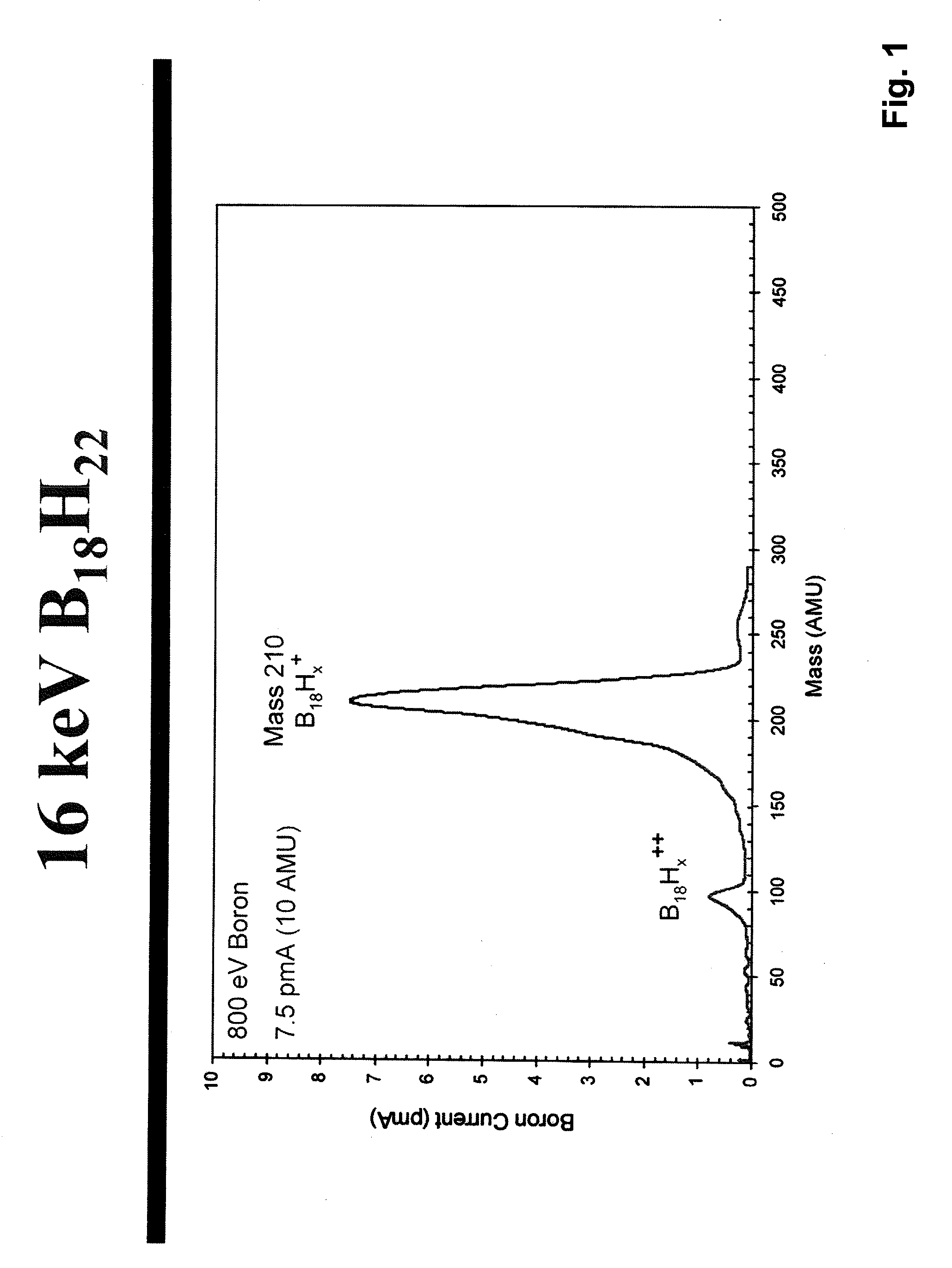
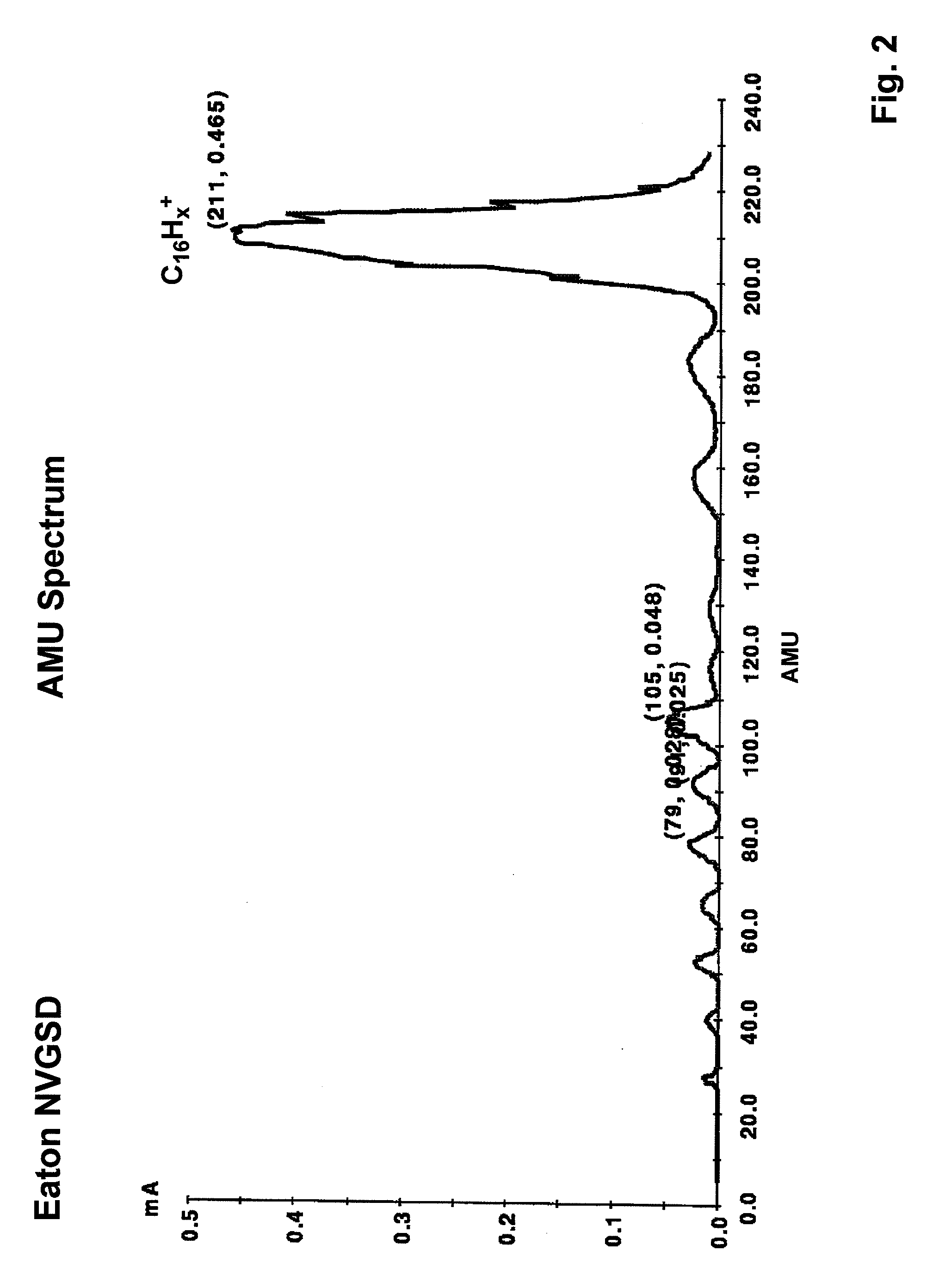
[0068]FIG. 1 shows a mass spectrum of B18H22 as produced by an ion implantation system. A ClusterIon® source, for example, as mentioned above, is used to generate ions which are extracted at 20 kV and transported through an analyzer magnet. A resolving aperture at the exist of the magnet provided a modest mass resolution of M / ΔM=15; the beam is scanned across the resolving aperture and the ion current is passed the resolving aperture and measured by a Faraday located about 2 meters from the source. The parent peak at 210 amu is composed of B18HX+; there is a range of retained H atoms of perhaps 10≦x≦22 which broadens the peak. The y-axis of the plot is the beam current multiplied by 18 (since there are 18 boron atoms per unit charge), so that the Faraday current was about 400 uA at mass 210. The effective boron implant energy is about 20 kV / 20 (since the average natural abundance boron mass is 10.8 amu and the ion mass about 210 amu)=1 keV per boron atom in the cluster. FIG. 2 shows...


PUM


Abstract

A process is disclosed which incorporates implantation of a carbon cluster into a substrate to improve the characteristics of transistor junctions when the substrates are doped with Boron and Phosphorous in the manufacturing of PMOS transistor structures in integrated circuits. There are two processes which result from this novel approach: (1) diffusion control for USJ formation; and (2) high dose carbon implantation for stress engineering. Diffusion control for USJ formation is demonstrated in conjunction with a boron or shallow boron cluster implant of the source / drain structures in PMOS. More particularly, first, a cluster carbon ion, such as C16Hx+, is implanted into the source / drain region at approximately the same dose as the subsequent boron implant; followed by a shallow boron, boron cluster, phosphorous or phosphorous cluster ion implant to form the source / drain extensions, preferably using a borohydride cluster, such as B18Hx+ or B10Hx+. Upon subsequent annealing and activation, the boron diffusion is reduced, due to the gettering of interstitial defects by the carbon atoms.

Description

CROSS REFERENCE TO RELATED APPLICATIONS[0001]This application is related to and claims the benefit of U.S. Provisional Patent Application No. 60 / 748,797, filed on Dec. 9, 2005, hereby incorporated by reference.BACKGROUND OF THE INVENTION[0002]1. Field of the Invention[0003]The present invention relates to a method of semiconductor manufacturing and more particularly to a method for implantation of carbon-containing clusters into a substrate for stress engineering and diffusion control to improve the characteristics of[0004]2. Description of the Prior ArtThe Ion Implantation Process[0005]The fabrication of semiconductor devices involves, in part, the formation of transistor structures within a silicon substrate by ion implantation. As disclosed by Sferlazzo et. al. in U.S. Pat. No. 5,497,006, ion implantation equipment includes an ion source which creates a stream of ions containing a desired dopant species, a beam line which extracts and accelerates the ions from the ion source by m...

Claims


Application Information

Patent Timeline
Patent Type & Authority Applications(United States)
IPC IPC(8): H01L21/8238H01L21/265H01L21/322H01L21/762
CPCH01L21/26506H01L21/26513H01L21/2658H01L21/823814H01L29/7848H01L29/165H01L29/6659H01L29/7833H01L21/823842H01L21/26566H01L21/265H01L21/425
Inventor KRULL, WADE A.HORSKY, THOMAS N.
Owner SEMEQUIP
Why Eureka
Try Eureka