Apparatus for characterization of thin film properties and method of using the same

a thin film and characterization technology, applied in the field of apparatus and thin film characterization, can solve the problems of limited commercial success of thin film photovoltaics at present, and high cost of pv modules, and achieve the effect of fast data acquisition speed

Inactive Publication Date: 2010-01-07
PHYSTECH
View PDF0 Cites 26 Cited by
  • Summary
  • Abstract
  • Description
  • Claims
  • Application Information

AI Technical Summary

Benefits of technology

[0040]It is an object of the present invention to provide a practical method and apparatus for high-speed characterization of thin film structures for such applications as, for a nonlimiting example, in-line manufacturing diagnostics of solar cell and flat panel display production lines. More particularly, it is an object of the present invention to provide an imaging ellipsometric and or polarimetric system with no mechanical scanning or rotation, or electro-optical tuning by employing hyper-spectral polarimetric imaging technique. It is another object of the present invention to provide a method of using the thin film characterization system of the present invention. The methods and apparatus of the present invention may be used to characterize the thickness, dispersion of refractive index and absorption coefficient of individual layers in multilayer thin film structure (and through that to provide the estimate on composition of said layer), interface roughness and stress distribution on at least one region over the sample surface at a single “shot” (i.e., from the single captured image). The very fast data acquisition speed of the system of present invention makes it particularly well suited for applications requiring high speed characterization, such as in-line manufacturing process control applications. Further, the present invention provides a thin film characterization system that is capable of detecting temporal and spatial variations of the device under test, such as solar cell structure during the processing, providing the opportunity for active adjustment of the processing conditions (closed-loop control). In addition to in-line manufacturing diagnostic and quality control the system and method of the present invention can be used in such nonlimiting applications as characterization of the biological and chemical samples, semiconductor processing, interference filter fabrication to name a few.
[0074]According to the second embodiment of the present invention the data processing means comprises reconstructing spatio-spectro-polarimetric distribution of the reflectivity from the DUT. The reconstruction of the spatio-spectro-polarimetric distribution of the reflectivity can comprise the steps of computer tomographic hyperspectral reconstruction and polarimetric reconstruction. The computer tomographic hyperspectral reconstruction can be performed by using MART, Expectation Maximization algorithm, heuristic algorithm or any other algorithm known to those skilled in the art. Polarimetric reconstruction can be performed by steps of inverse Fourier transform, filtering the transformed data array and Fourier transform of the filtered data in the spatial domain. Further mathematical processing may be performed as well (such as normalization by the reference spectrum, smoothing, fitting, etc). The reconstructed data will thus provide the means for further processing to identify the structural parameters of the DUT.
[0077]The method and apparatus of the present invention are broadly applicable for characterization, quality control and manufacturing diagnostics of the thin film structures. The present method is particularly useful for in-line manufacturing diagnostics and control of solar cell, flat panel displays and semiconductor devices, where high speed characterization tool is required to meet the manufacturing process throughput. The advantage of the method and apparatus of the present invention is that they provide high-throughput, high accuracy / high resolution technique for thin film characterization.

Problems solved by technology

The main obstacle for widespread use of PV energy at present is the higher cost of PV energy compared to that of fossil energy, resulting at large, from the high cost of PV modules.
For example, commercial success of thin film photovoltaics at present is limited by performance and cost, the factors that are typically interrelated and negatively impacted by the lack of reliable and accurate process monitoring and control.
At present, diagnostic capabilities for thin film PV manufacturing are rudimentary, and manufacturers can only assess their product after module completion.
This makes the development of PV manufacturing diagnostic systems a serious challenge.
It is impossible to measure all the critical parameters of the solar cell with a apparatus based on a single physical phenomenon.
Unfortunately, such a technique is incapable of providing any relevant information for multilayer structures, such as refractive indices or stresses in individual layers.
However, spectroscopic ellipsometry technique is slow because provides only single-point information, thus incompatible with efficient in-line diagnostics (state of the art systems offer the throughput of ˜1 wafer / minute compared to less than a wafer / second throughput requirement).
A number of other methods have been proposed to solve this problem, but none of them is practical enough (fast, accurate and capable of providing sufficient information) to permit effective in-line PV manufacturing diagnostic.
Still, said U.S. Pat. No. 5,872,630 fails to disclose the system capable of measurements of DUT in more than one point at a time.
As with previously discussed inventions, these disclosures also fail to provide the measurements over the multiple spatial points of the DUT at a time.
As mentioned previously in this disclosure, the known to those skilled in the art spectroscopic ellipsometry systems, while providing wealth of information on the multilayer thin film structures (for a nonlimiting example, solar cell structures), are often too slow for the use in effective in-line manufacturing diagnostics.
Such a system still has a number of important drawbacks: 1) the filter wheel assembly makes system mechanically complex and thus expensive, 2) the spectral resolution of the system is limited by the quantity and optical characteristics of filter system, and, most importantly for thin film in-line characterization, 3) the sampling rate of the system is limited by mechanical rotation of the filter wheel and is in a range of few seconds to few tens of the seconds, thus not fast enough for many in-line manufacturing diagnostic applications, such as, for a nonlimiting example, manufacturing of solar cells or flat panel displays.
The H-matrix is determined during calibration, so the problem of tomographic hyperspectral imager is to reconstruct the vector f from measured g and known H. The direct inversion of (2) is often ill-posed, so other methods of hypercube (cubic portion of the spatio-spectral space) reconstruction are used for these purposes.
It is also should be noted that as disclosed in the referenced previously papers, this technique may not be extended to such applications because of the following deficiencies / omitted subjects: 1) to realize thin film characterization and in-line manufacturing control system one needs to add illumination system with proper spectral and polarization properties; 2) the calibration technique, employed in U. Arizona experiments (mechanical scanning of the fiber coupled to a monochromator in the object plane) is very time consuming and hardly practical in the field, 3) hypercube reconstruction algorithm is very time consuming and is not fast enough to such applications as solar cell or flat panel display manufacturing in-line diagnostics.
The deficiency of such a technique for thin film characterization is the absence of the spectral data which would provide very poor estimation of the thin film sample structure, thus making it not well suited for the thin film characterization and processing control applications.

Method used


Image

  • Apparatus for characterization of thin film properties and method of using the same
  • Apparatus for characterization of thin film properties and method of using the same
  • Apparatus for characterization of thin film properties and method of using the same

Examples


first embodiment

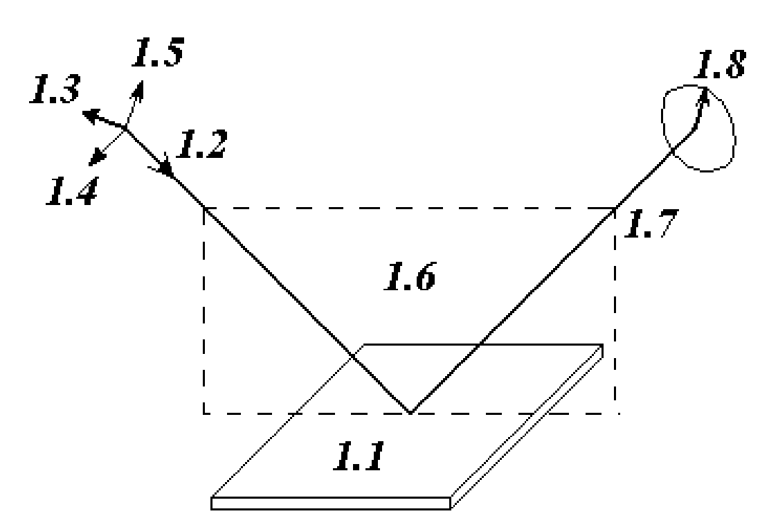
[0092]The thin film characterization apparatus according to the present invention is illustrated by an exemplarily nonlimiting FIG. 7. It comprises:[0093]a) a broadband light source (component 1 in FIG. 7),[0094]b) an optical assembly (component 2 in FIG. 7) for delivery of light emitted by said light source to the first polarization assembly,[0095]c) a first polarization assembly (components 3,4 in FIG. 7) for defining the state of polarization of the light emitted by said light source,[0096]d) a device under test (component 6 in FIG. 7) illuminated by light emitted by said light source with polarization state defined b y the first polarization assembly which modifies the spectral and polarization content of the reflected light in response to the structure of said device under test,[0097]e) an optical assembly (component 7 in FIG. 7) for delivery of light reflected from device under test to the second polarization assembly,[0098]f) a second polarization assembly (components 8, 9, 1...

second embodiment

[0111]The thin film characterization apparatus according to the present invention is illustrated by an exemplarily nonlimiting FIG. 8. It comprises:[0112]a) a broadband light source (component 1 in FIG. 8),[0113]b) an optical assembly (component 2 in FIG. 8) for delivery of light emitted by said light source to the first polarization assembly,[0114]c) a first polarization assembly (components 3 and 4 in FIG. 8) for defining the state of polarization of the light emitted by said light source,[0115]d) a device under test (component 6 in FIG. 8) illuminated by light emitted by said light source with polarization state defined b y the first polarization assembly which modifies the spectral and polarization content of the reflected light in response to the structure of said device under test,[0116]e) an optical assembly (component 7 in FIG. 8) for delivery of light reflected from device under test to the second polarization assembly,[0117]f) a second polarization assembly (components 8, ...

fourth embodiment

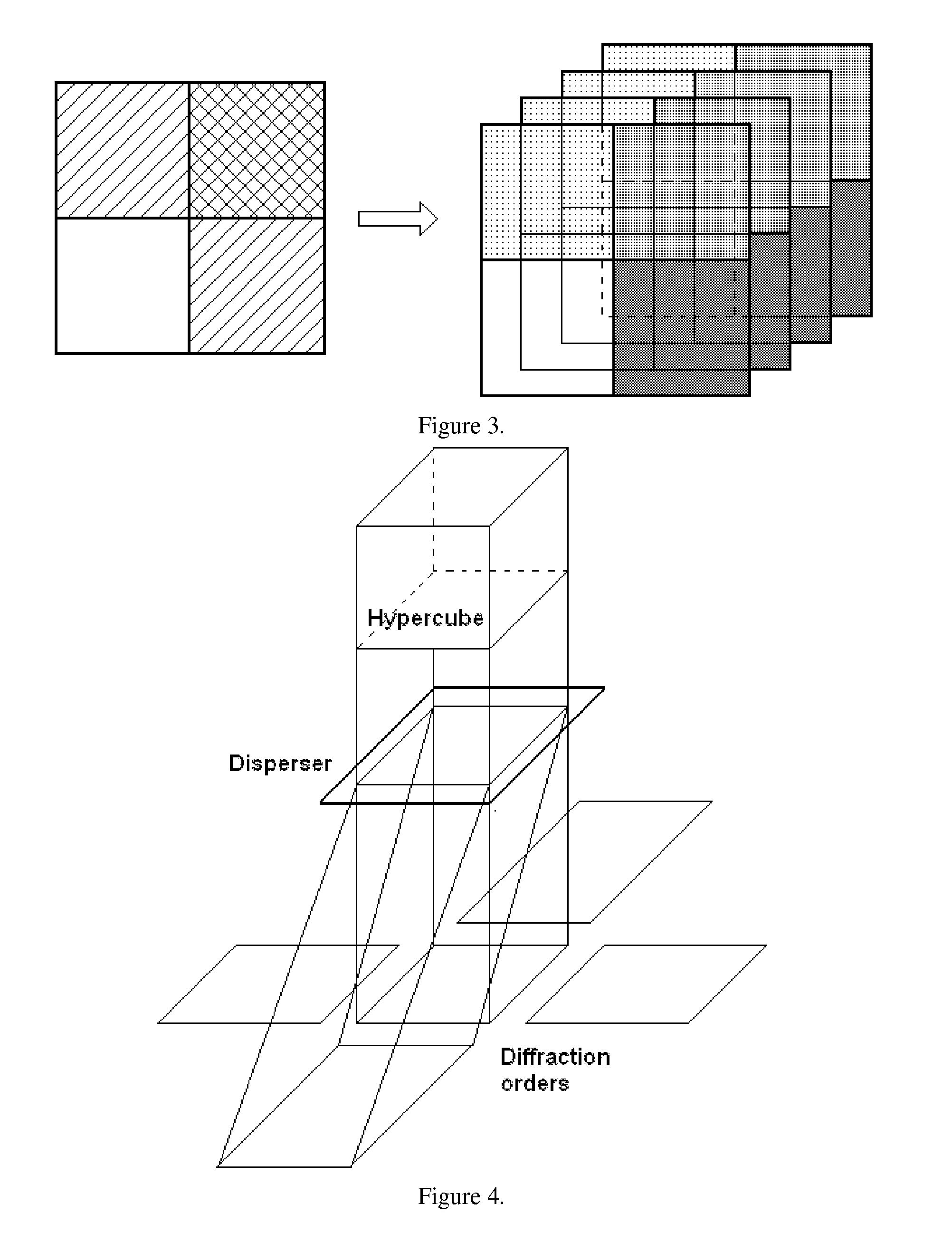
[0134]The basis of the approach that is behind such a method of the present invention is the fact that the spatio-spectro-polarimetric anomaly in the hypercube manifests itself as intensity peculiarities in thin film characterization apparatus' nonreconstruced image as well, as schematically illustrated in calculated FIG. 12. Hence, in principle, the anomalies can be detected from the statistical analysis of the nonreconstructed raw image without the computationally-intense full hypercube restoration. To accomplish it one will need to statistically analyze the nonreconstructed raw images and identify the anomalies in intensity distribution (with mathematical processing and optionally buy mathematically comparing the raw data with preliminary stored reference data); selectively reconstruct the hypercube portions in areas of detected anomalies (highlighted in FIG. 12), and detect anomalies in the reconstructed hypercube portions and identify the nature of anomalies. Implementation of ...


PUM


Abstract

This invention provides an apparatus and method for characterization of thin film structures. More particularly, the present invention provides methods and devices for fast and accurate identification of optical constants, thickness, interface roughness and stresses of a sensing film structures by spectropolarimetric imaging technique. This invention also provides the method for active in-line manufacturing diagnostics and process control. The invention is broadly applicable with most important applications being manufacturing diagnostics, process control, quality control and characterization of solar cells, flat panel displays and semiconductor structures.

Description

CROSS-REFERENCES TO RELATED APPLICATIONS[0001]The present non-provisional application relates to previously filed provisional application No. 61 / 077,482 with filing date Jul. 1, 2008STATEMENT REGARDING FEDERALLY SPONSORED RESEARCH OR DEVELOPMENT[0002]Not applicable.FIELD OF THE INVENTION[0003]The present invention relates to an apparatus and method for thin film characterization. In more detail, the present invention is related to the apparatus and method for measuring the spectral dependences of refractive indices, thicknesses, birefringence and / or interface roughness of thin film structures through the use of hyperspectral imaging. The apparatus and method of present invention can be applied for thin film characterization quality control and in-situ process monitoring. In-line manufacturing diagnostics of solar cells is one of the preferred applications of the technology disclosed in present invention.BACKGROUND OF THE INVENTION[0004]Photovoltaic (PV) technology is predicted to ha...

Claims


Application Information

Patent Timeline
Patent Type & Authority Applications(United States)
IPC IPC(8): G06F19/00G01J3/447
CPCG01J3/2823G01N2021/213G01N21/211G01J3/447
Inventor KOCHERGIN, VLADIMIR
Owner PHYSTECH
Why Eureka
Try Eureka