Vibration sensor and method for manufacturing the vibration sensor

Active Publication Date: 2010-02-18
MMI SEMICON CO LTD
View PDF11 Cites 13 Cited by
  • Summary
  • Abstract
  • Description
  • Claims
  • Application Information

AI Technical Summary

Benefits of technology

[0011]In view of the technical problems described above, it is an object of the present invention to provide a vibration se

Problems solved by technology

Thus, the opening area at the back side of the through-hole becomes large compared to the area of the diaphragm, and miniaturization of the capacitor microphone is difficult.
If the thickness of the semiconductor substrate is reduced, the ratio of the opening area of the back surface with respect to the opening area of the front surface of the through-hole can be reduced, but the strength of the semiconductor substrate lowers and handling at the time of manufacturing becomes difficult, and thus reducing the thickness of the semiconductor substrate has limits.
However, in devices of DRIE, ICP, and the like, a price of the device is high and processing of a wafer is in sheet form, and thus productivity is no

Method used


Image

  • Vibration sensor and method for manufacturing the vibration sensor
  • Vibration sensor and method for manufacturing the vibration sensor
  • Vibration sensor and method for manufacturing the vibration sensor

Examples


first embodiment

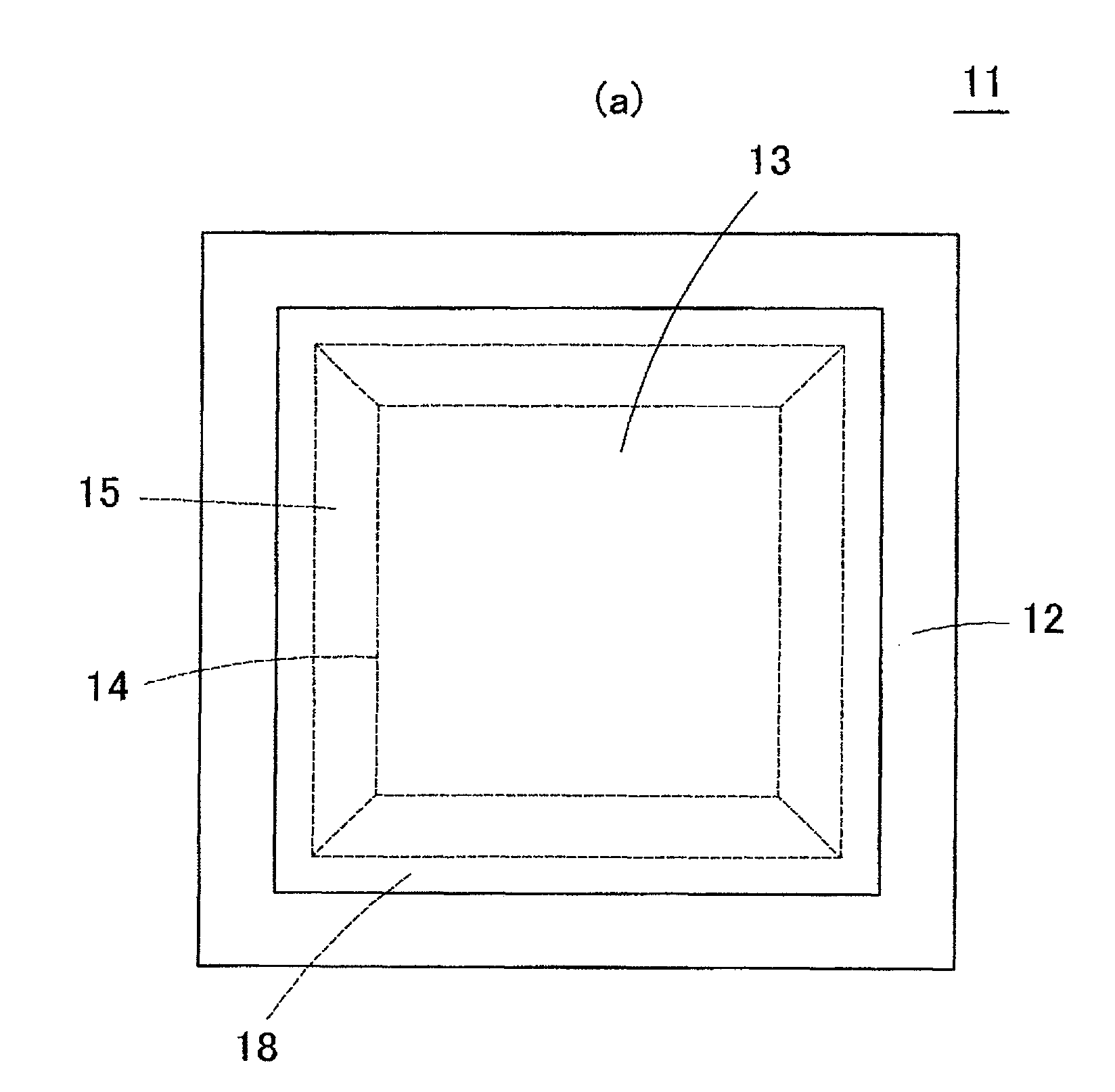
[0077]FIG. 1(a) is a plan view showing a structure of a vibration sensor 11 according to a first embodiment of the present invention, and FIG. 1(b) is a cross-sectional view thereof. The vibration sensor 11 is used in an acoustic sensor such as a semiconductor microphone and an ultrasonic sensor, a thin film filter, and the like. The vibration sensor 11 includes an Si substrate 12, and a thin film 13 (diaphragm). The Si substrate 12 is a (100) plane substrate. The Si substrate 12 is etched from the back side so as to form a rectangular through-hole 14, which is passed through from the front to the back and which side in each horizontal and vertical direction lies in the (110) direction. The through-hole 14 has inclined surfaces 15, 17 formed on the front side and the back side by a (111) plane or a crystal plane equivalent thereto, and a vertical surface 16 is formed between the inclined surfaces 15, 17. The vertical surface 16 is actually configured by a plurality of crystal planes...

second embodiment

[0095]FIG. 5(a) is a plan view showing a vibration sensor 31 according to the second embodiment of the present invention, and FIG. 5(b) is a cross-sectional view thereof. In the vibration sensor 31, the thin film 13 of polycrystalline silicon is formed on the Si substrate 12 so as to cover the upper surface of the through-hole 14. The thin film 13 has the lower surface of the outer peripheral part supported by the holder 18 at the upper surface of the Si substrate 12 and is lifted from the upper surface of the Si substrate 12, where a region surrounded by the holder 18 is deformable.

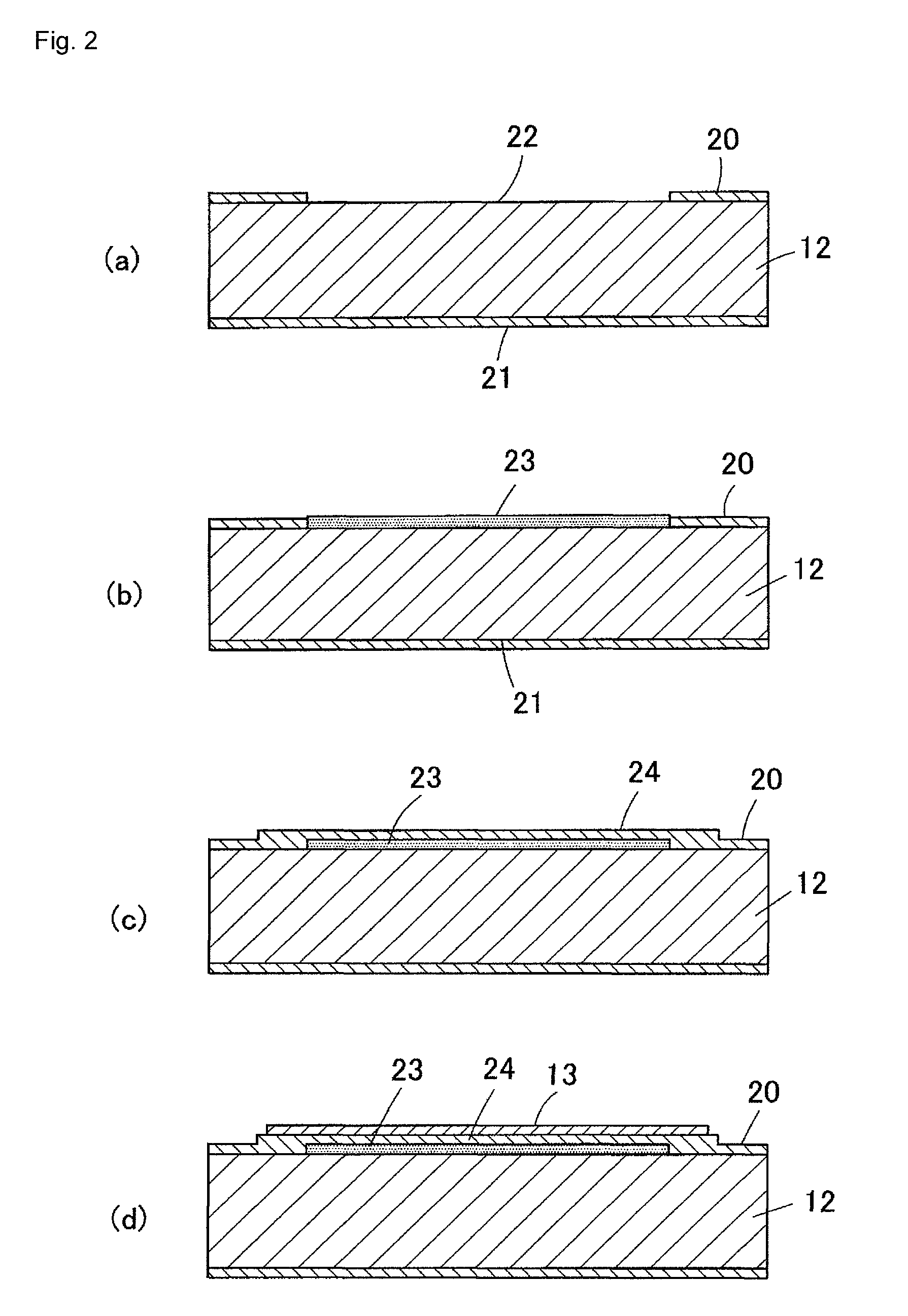
[0096]FIGS. 6(a) to (d) and FIGS. 7(a) to (d) are cross-sectional views describing the manufacturing steps of the vibration sensor 31. The manufacturing steps of the vibration sensor 31 will be described below according to FIGS. 6(a) to (d) and FIGS. 7(a) to (d).

[0097]First, after forming the SiO2 thin film on the upper surface of the Si substrate 12, the unnecessary portion of the SiO2 thin film is remo...

third embodiment

[0108]FIG. 8(a) is a plan view showing a structure of a vibration sensor 41 according to the third embodiment of the present invention, and FIG. 8(b) is a cross-sectional view taken along line X-X of FIG. 8(a). The vibration sensor 41 has a corrugated structure and a functional portion such as a stopper 43 arranged in the thin film 13.

[0109]The corrugated structure of the thin film 13 is configured by two bent portions 42 having a square annular shape. Each bent portion 42 is bent such that the cross-section thereof projects to the upper side of the thin film 13. It has been reported in “The fabrication and use of micromachined corrugated silicon diaphragms” (J. H. Jerman, Sensors and Actuators A21-A23 pp. 998-992, 1992) that a displacement of the thin film 13 increases and a deflection by stress reduces by forming the corrugated structure in the thin film 13.

[0110]The stopper 43 is formed by projecting the front surface of the thin film 13 to a round projection shape. In a case of ...


PUM


Abstract

A method for manufacturing a vibration sensor including forming a sacrifice layer at one part of a front surface of a semiconductor substrate of monocrystalline silicon with a material isotropically etched by an etchant for etching the semiconductor substrate, forming a thin film protective film with a material having resistance to the etchant on the sacrifice layer and the front surface of the semiconductor substrate at a periphery of the sacrifice layer, forming a thin film of monocrystalline silicon, polycrystalline silicon, or amorphous silicon on an upper side of the sacrifice layer, opening a backside etching window in a back surface protective film having resistance to the etchant for etching the semiconductor substrate formed on a back surface of the semiconductor substrate, forming a through-hole in the semiconductor substrate by etching the semiconductor substrate anisotropically by using crystal-oriented etching by applying the etchant from the back surface window, then etching the sacrifice layer isotropically by the etchant after the etchant reaches the front surface of the semiconductor substrate, and then etching the semiconductor substrate anisotropically by using crystal-oriented etching from a front side by the etchant spread to a space formed after the sacrifice layer is removed, and forming a holder for supporting the thin film on an upper surface of the semiconductor substrate by removing the thin film protective film partially.

Description

TECHNICAL FIELD[0001]The present invention relates to a vibration sensor and a method for manufacturing the same, in particular, to a vibration sensor including a thin film such as a diaphragm and a method for manufacturing the same.BACKGROUND ART[0002]A vibration sensor in which a thin film is formed by stacking layers of monocrystalline silicon or polycrystalline silicon on a silicon substrate, and the thin film is used as a diaphragm, is being developed by applying a semiconductor integrated circuit manufacturing technique. The diaphragm made of silicon has a small internal stress and a low density compared to metal such as aluminum and titanium, and thus a vibration sensor of high sensitivity can be obtained and compliance with a semiconductor integrated circuit manufacturing step is also satisfactory. The vibration sensor including such a diaphragm includes a capacitor microphone disclosed in Patent Document 1. In such a capacitor microphone, a diaphragm (movable electrode) and...

Claims


Application Information

Patent Timeline
IPC IPC(8): H01L29/84H01L21/28
CPCB81B2201/0257B81B2203/0127B81B2203/0353B81B2201/0285H04R19/005H04R19/04B81C1/00182H01L29/84H01L21/306
Inventor KASAI, TAKASHIHORIMOTO, YASUHIROKATO, FUMIHITOMUNECHIKA, MASAKIWAKABAYASHI, SHUICHITAKAHASHI, TOSHIYUKIINUGA, MASAYUKI
Owner MMI SEMICON CO LTD
Why Eureka
Try Eureka