Connecting terminal, semiconductor package using connecting terminal and method for manufacturing semiconductor package

Inactive Publication Date: 2010-03-25
HITACHI CHEM CO LTD
View PDF6 Cites 74 Cited by
  • Summary
  • Abstract
  • Description
  • Claims
  • Application Information

AI Technical Summary

Benefits of technology

[0030]According to the invention it is possible to improve the connection reliability of connecting terminals having displacemen

Problems solved by technology

However, with the increasing high density of wirings due to smaller semiconductor packages, it is becomi

Method used


Image

  • Connecting terminal, semiconductor package using connecting terminal and method for manufacturing semiconductor package
  • Connecting terminal, semiconductor package using connecting terminal and method for manufacturing semiconductor package
  • Connecting terminal, semiconductor package using connecting terminal and method for manufacturing semiconductor package

Examples


Example

Example 1

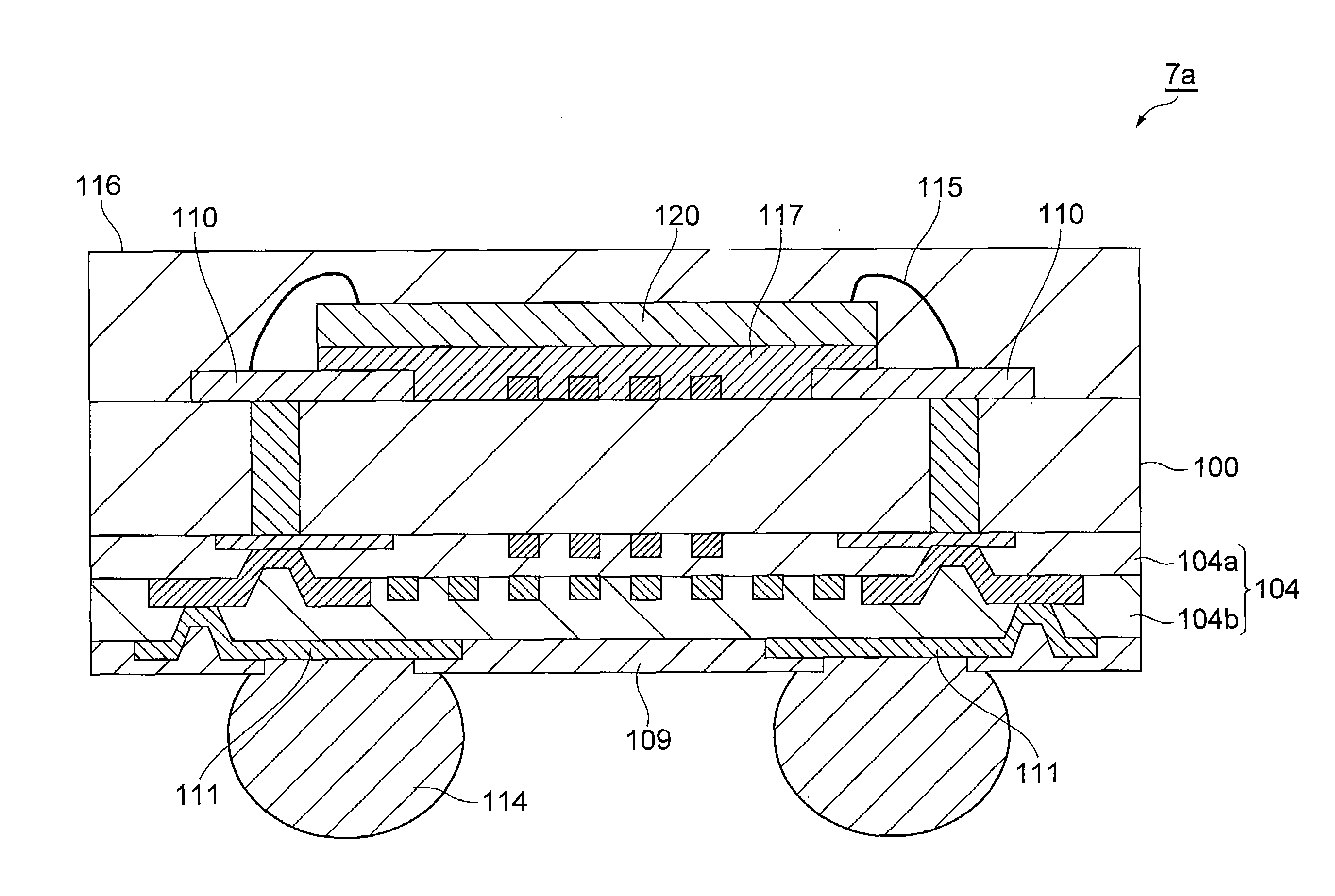
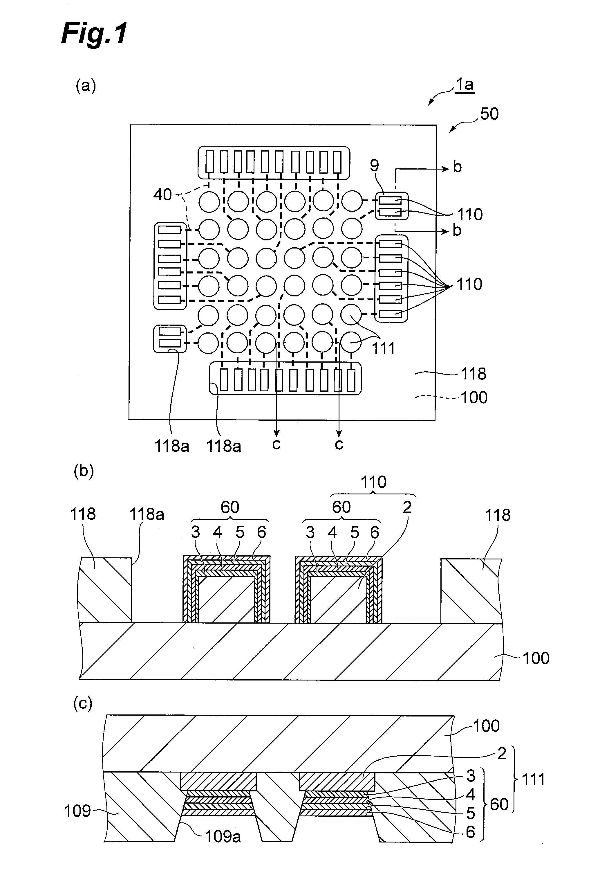
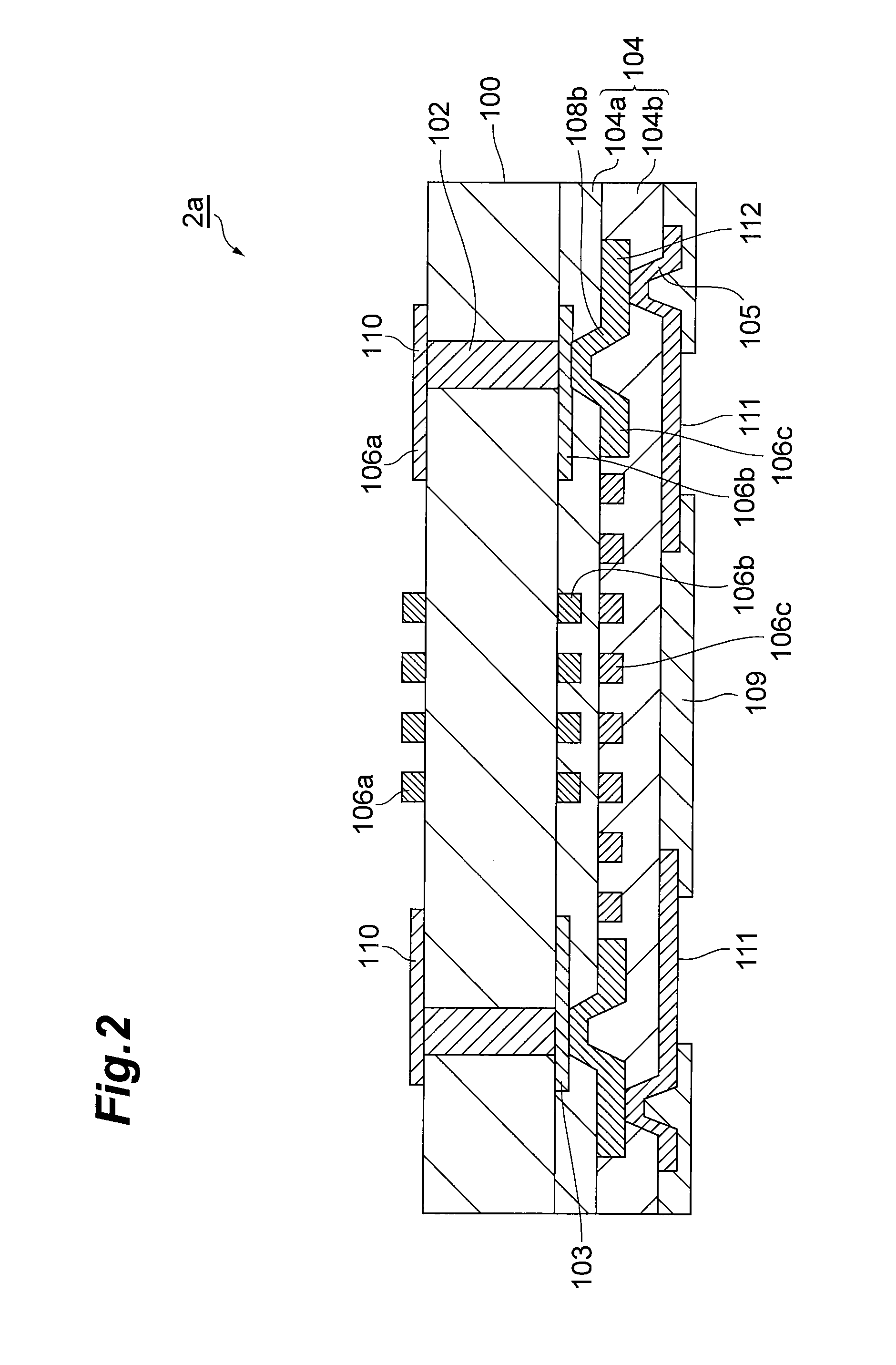
[0177]The following steps were carried out to fabricate a semiconductor chip mounting board having the same construction as the embodiment shown in FIG. 2, according to the manufacturing method embodiment shown in FIG. 6.

[0178](Step a: Formation of First Wiring)

A 0.4 mm-thick soda glass board (thermal expansion coefficient: 11 ppm / ° C.) was prepared as the core board 100, and a 200 nm copper thin-film was formed on one side thereof by sputtering (hereinafter this will be referred to as the “first main side”). The sputtering was carried out using a sputtering apparatus (MLH-6315, product of ULVAC Corp.) under the following conditions 1. In addition, a copper plating layer with a film thickness of 10 μm was formed by electrolytic copper plating on the copper thin-film. An etching resist was then formed to cover the sections of the copper plating layer which were to constitute the wiring, and a ferric chloride etching solution was used for etching to form first wiring 106a (in...

Example

Example 2

[0204]Each step was carried out in the same manner as Example 1, except that step m of Example 1 was omitted. The results are shown in Table 1.

Example

Examples 3-8

[0205]The immersion treatment time for structure 6g-j and / or structure 6g-k in step j and / or step k of Example 1 was changed as shown in Table 1, to form electroless palladium plating films with different film thicknesses on the connecting terminals and wiring of structure 6g-j and the connecting terminals and wiring of wiring structure 6g-k. The other steps were carried out in the same manner as Example 1. The results are shown in Table 1.


PUM

PropertyMeasurementUnit
Percent by massaaaaaaaaaa

Abstract

The connection reliability of connecting terminals with displacement gold plating films is improved by connecting terminals comprising a conductive layer, an electroless nickel plating film, a first palladium plating film which is a displacement or electroless palladium plating film with a purity of 99% by mass or greater, a second palladium plating film which is an electroless palladium plating film with a purity of at least 90% by mass and less than 99% by mass, and a displacement gold plating film, wherein the electroless nickel plating film, the first palladium plating film, the second palladium plating film and the displacement gold plating film are laminated in that order on one side of the conductive layer, and the displacement gold plating film is situated on the uppermost surface layer on the opposite side from the conductive layer.

Description

TECHNICAL FIELD[0001]The present invention relates to a connecting terminal, a semiconductor package using a connecting terminal, and a method for manufacturing a semiconductor package.BACKGROUND ART[0002]In recent years, advancements have continued to be made in size and weight reduction, high performance and high functionality of devices such as personal computers, cellular phones, wireless base stations, optical communication devices, servers and routers, of various sizes. Development of high-density mounting techniques for System-on-Chips (SoC) and System-in-Packages (SiP) is also progressing with increasing LSI speeds and functionality for CPU, DSP and memory devices.[0003]Build-up system-type multilayer circuit boards are therefore being employed on semiconductor chip mounting boards and motherboards. With advancements in mounting technologies such as multi-pin and narrow-pitch formation on packages, printed circuit boards have been shifting from QFP (Quad Flat Package) to BGA...

Claims


Application Information

Patent Timeline
IPC IPC(8): H01L23/498H01B1/02H01L21/60
CPCC23C18/1651C23C18/1837C23C18/42C23C18/54H01L21/4846H01L21/561H01L23/3128H01L23/498H01L23/49816H01L23/49822H01L23/49838H01L23/544H01L24/16H01L24/32H01L24/49H01L24/81H01L24/97H01L2223/54426H01L2223/5446H01L2224/13099H01L2224/16225H01L2224/32057H01L2224/32225H01L2224/48091H01L2224/48227H01L2224/49H01L2224/73204H01L2224/73265H01L2224/81121H01L2224/81801H01L2224/83385H01L2224/97H01L2924/01002H01L2924/01003H01L2924/01004H01L2924/01005H01L2924/01006H01L2924/01007H01L2924/01011H01L2924/01013H01L2924/01014H01L2924/01015H01L2924/01016H01L2924/01018H01L2924/01022H01L2924/01027H01L2924/01028H01L2924/01029H01L2924/0103H01L2924/01031H01L2924/01032H01L2924/01033H01L2924/0104H01L2924/01042H01L2924/01046H01L2924/01047H01L2924/01049H01L2924/0105H01L2924/01057H01L2924/01061H01L2924/01073H01L2924/01074H01L2924/01078H01L2924/01079H01L2924/01082H01L2924/01083H01L2924/01088H01L2924/01322H01L2924/09701H01L2924/10329H01L2924/15311H05K3/244H05K2203/072H05K2203/073H01L24/48H01L2924/01019H01L2924/01023H01L2924/01024H01L2924/01041H01L2924/01044H01L2924/01045H01L2924/014H01L2924/0132H01L2924/0133H01L2224/45144H01L2924/1579H01L2224/29111H01L2224/2919H01L2224/13111H01L2224/45015H01L2924/00014H01L2924/00H01L2924/3512H01L2924/00012H01L24/45H01L24/73H01L2924/00011H01L2924/12044H01L2924/15787H01L2924/15788H01L2924/181H01L2924/351H01L2924/20752H01L2924/00015H01L2224/05599H01L2224/0401C23C18/52H01L23/12
Inventor EJIRI, YOSHINORIHATAKEYAMA, SHUICHIARIKE, SHIGEHARUHASEGAWA, KIYOSHI
Owner HITACHI CHEM CO LTD
Why Eureka
Try Eureka