

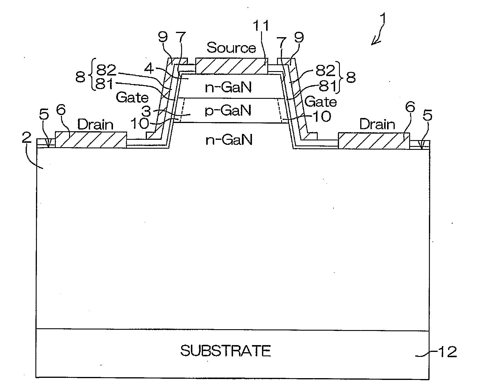
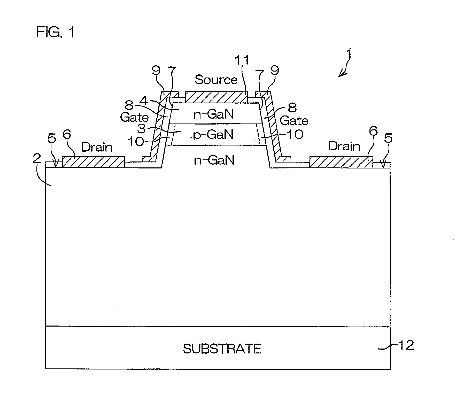
Nitride semiconductor device, nitride semiconductor package, and method for manufacturing nitride semiconductor device
a technology of nitride semiconductor and semiconductor device, which is applied in the direction of semiconductor device, semiconductor/solid-state device details, electrical apparatus, etc., can solve the problems of increased gate threshold value voltage, device is not always suitable for power device, and device cannot be used for power device operation. , to achieve the effect of preventing the possibility of reaching through breakdown, and increasing the gate withstand voltag
- Summary
- Abstract
- Description
- Claims
- Application Information
AI Technical Summary
Benefits of technology
Problems solved by technology
Method used
Image

Examples
example 1
The Surface of the P-Type Nitride Semiconductor Layer is Applied with a Process for Rendering an N-Type
[0237]The p-type impurity concentration in the p-type nitride semiconductor layer: 1018 / cm3
[0238]The conductive characteristics of the channel forming region: n-type[0239](film thickness of the channel forming region having an n-type impurity concentration of 1018 / cm3: 0.025 μm)
[0240]Film thickness of the gate insulating film: 500 Å
example 2
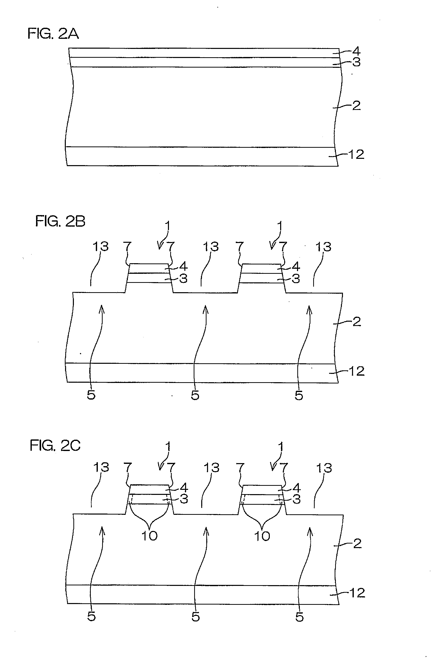
[0247]On the substrate, a GaN nitride semiconductor laminated structure formed of an npn laminated structure (an n-type GaN layer, a p-type GaN layer, and an n-type GaN layer were laminated in order) was formed by a metal organic chemical vapor deposition method (MOCVD method), and thereafter, SiO2 was film-deposited for 350 nm at an upper section of the n-type GaN layer of the topmost surface by a magnetron sputtering method. Subsequently, a resist was applied on this SiO2, and patterned by a well-known photolithography technique. By dry-etching using CF4, the SiO2 was selectively etched. Thereafter, the resist was removed by ashing.
[0248]After the removal of the resist, dry-etching using Cl2 / SiCl4 was adopted to selectively etch GaN. Thereafter, the SiO2 was removed by BHF.
[0249]Subsequently, the substrate formed thereon with the GaN nitride semiconductor laminated structure was put in an ECR (Electron Cyclotron Resonance) deposition apparatus, and the target (Si) was irradiated w...
example 3
[0251]Except that the SiO2 film (gate insulating film) was formed by a magnetron sputtering method, the field effect transistor was fabricated by a method similar to that in Example 2. Upon the formation of the SiO2 film by a magnetron sputtering method, a substrate formed thereon with the GaN nitride semiconductor laminated structure was first put in a counter electrode type apparatus, and within the counter electrode type apparatus, an Ar+ plasma was produced. Subsequently, the target (SiO2) was applied with a voltage of 300 V, and the target was irradiated with the produced Ar+ plasma. Thereby, the SiO2 was sputtered to form the SiO2 film (gate insulating film) on the surface of the GaN nitride semiconductor laminated structure. At this time, oxygen was pushed out from the target, and implanted to the p-type GaN layer by energy of 300 eV. Thereby, on the surface of the p-type GaN layer, a region made of a semiconductor (rendered n-type) was formed.
PUM
| Property | Measurement | Unit |
|---|---|---|
| angle | aaaaa | aaaaa |
| thickness | aaaaa | aaaaa |
| gate threshold value voltage | aaaaa | aaaaa |
Abstract
Description
Claims
Application Information