Display device
a display device and display portion technology, applied in semiconductor devices, instruments, electrical devices, etc., can solve the problems of not always suitable for a larger glass substrate, and achieve the effect of reducing the area occupied by the connection portion and reducing the size of the display devi
- Summary
- Abstract
- Description
- Claims
- Application Information
AI Technical Summary
Benefits of technology
Problems solved by technology
Method used
Image
Examples
embodiment 1
[0044]In this embodiment, an example of a display device including a pixel portion and a protective circuit which includes a non-linear element provided near the pixel portion is described with reference to drawings.
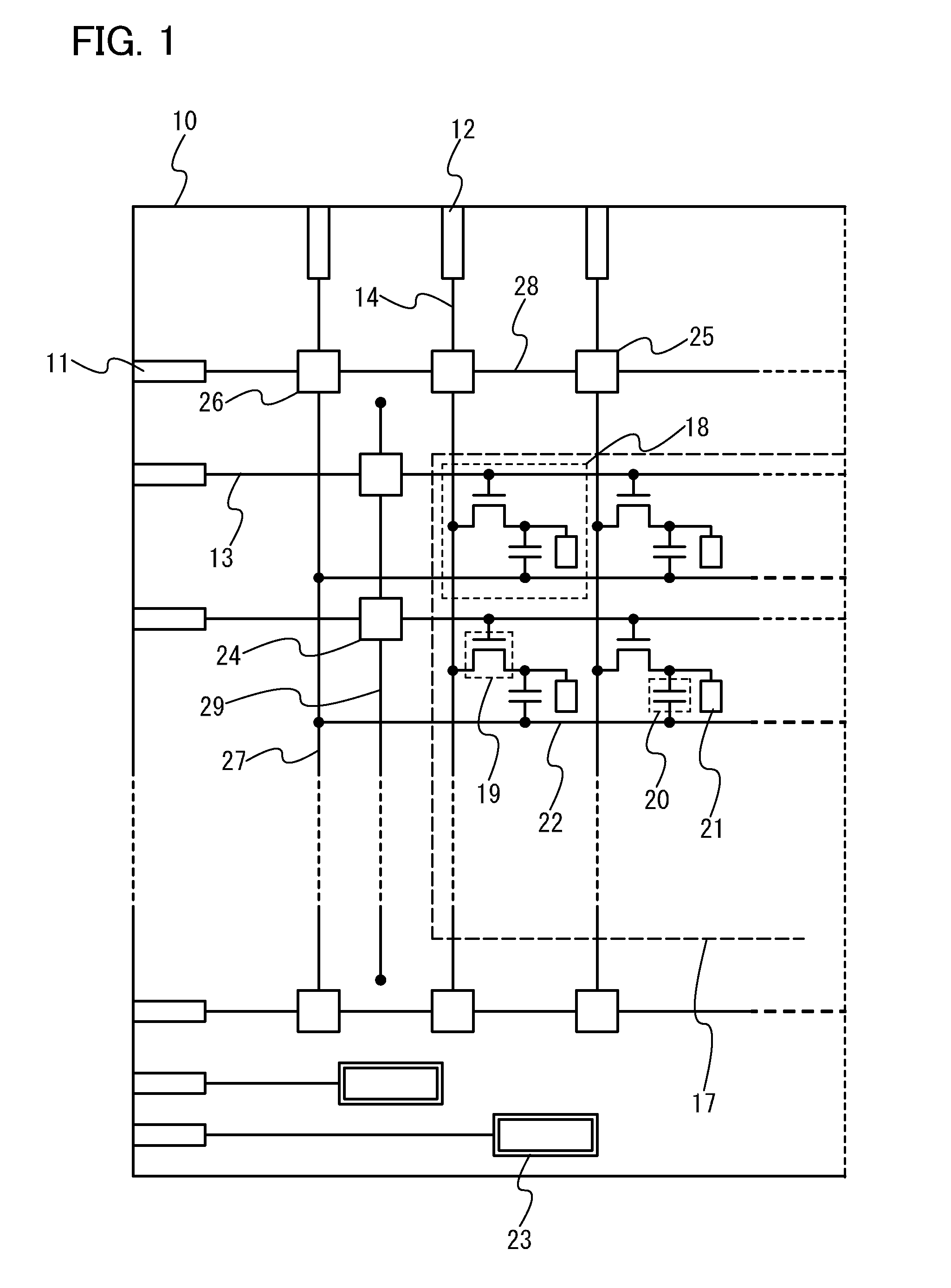
[0045]FIG. 1 illustrates a positional relationship among signal input terminals, scan lines, signal lines, protective circuits including non-linear elements, and a pixel portion in a display device. Over a substrate 10 having an insulating surface, scan lines 13 and signal lines 14 intersect with each other to form a pixel portion 17.
[0046]The pixel portion 17 includes a plurality of pixels 18 arranged in matrix. The pixel 18 includes a pixel transistor 19 connected to the scan line 13 and the signal line 14, a storage capacitor portion 20, and a pixel electrode 21.
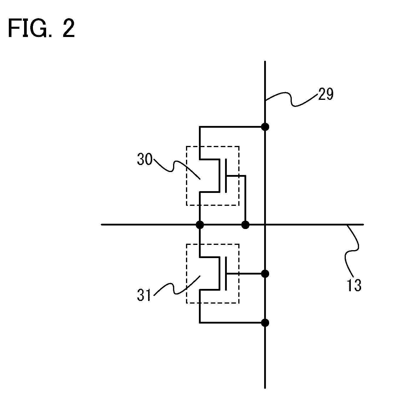
[0047]In the pixel structure illustrated here, one electrode of the storage capacitor portion 20 is connected to the pixel transistor 19 and the other electrode is connected to a capacitor line 22. Moreover, t...
embodiment 2
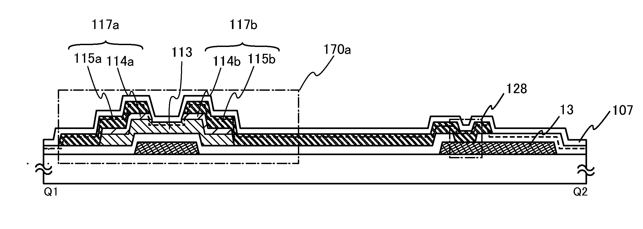
[0072]In this embodiment, an example of a process for manufacturing the protective circuit illustrated in FIG. 4A described in Embodiment 1 is described with reference to FIGS. 6A to 6C and FIGS. 7A to 7C. FIGS. 6A to 6C and FIGS. 7A to 7C are cross-sectional views taken along line Q1-Q2 of FIG. 4A.
[0073]In FIG. 6A, a glass substrate of barium borosilicate glass, aluminoborosilicate glass, aluminosilicate glass, or the like available in the market can be used as a substrate 100 having a light-transmitting property. For example, a glass substrate which includes more barium oxide (BaO) than boric acid (B2O3) in composition ratio and whose strain point is 730° C. or higher is preferable. This is because such a glass substrate is not strained even in the case where the oxide semiconductor layer is thermally processed at high temperatures of about 700° C.
[0074]Next, a conductive film which is to be a gate wiring including the gate electrode 111 and the scan line 13, a capacitor wiring, a...
embodiment 3
[0107]This embodiment describes an example of an electronic paper in which a protective circuit and a thin film transistor in a pixel portion are provided over one substrate, as a display device to which an embodiment of the present invention is applied.
[0108]FIG. 10 illustrates an active matrix electronic paper as an example of a display device to which an embodiment of the present invention is applied. A thin film transistor 581 used for a semiconductor device can be manufactured in a manner similar to the non-linear element described in Embodiment 2. The thin film transistor 581 has excellent electrical characteristics and includes a semiconductor layer including a semiconductor oxide containing In, Ga, and Zn.
[0109]The electronic paper of FIG. 10 is an example of a display device in which a twisting ball display system is employed. The twisting ball display system refers to a method in which spherical particles each colored in black and white are arranged between a first electro...
PUM
 Abstract
Description
Claims
Application Information


