Aluminum gallium nitride/gallium nitride high electron mobility transistors

Inactive Publication Date: 2010-04-08
THE HONG KONG UNIV OF SCI & TECH
View PDF61 Cites 49 Cited by
  • Summary
  • Abstract
  • Description
  • Claims
  • Application Information

AI Technical Summary

Benefits of technology

[0015]Thus, in further non-limiting embodiments, the provided structures can be combined with Low Density Drain (LDD) fabrication methods to provide a EBB/LDD combination HEMT (e.g., an EBB/LDD HEMT) heterostructure that can further improve the electric field distribution. Further non-limiting embodiments can include an EBB layer or region such that the EBB layer or region is extended substantially to the source region to further improve source-drain isolation in the HEMT “off-state.”
[0016]In addition, according to various aspects, fluorine ions can be introduced into the devices using one or more processes including plasma treatment, plasma immersion ion implantation,

Problems solved by technology

However, reported off-state breakdown voltage values still remain significantly below the theoretical limit for such devices.
As a result, it is expected that electrons can be injected from the source to the high-field region through the buffer and initiate impact ionization in the channel at large drain bias and cause the premature three-terminal off-state breakdown of the device before gate breakdown.
While a general reduction in n-type background doping in the unintentionally doped GaN buffer layer has been attempted,

Method used


Image

  • Aluminum gallium nitride/gallium nitride high electron mobility transistors
  • Aluminum gallium nitride/gallium nitride high electron mobility transistors
  • Aluminum gallium nitride/gallium nitride high electron mobility transistors

Examples


Example

Overview

[0049]As used herein, acronyms are used to denote the following: Source (S), Drain (D), Gate (G), Current (I), Voltage (V), Breakdown Voltage (BV), Transconductance (Gm), L (Length, Distance, or Spacing), X (Relative Position), Ohmic Contact (O), Anode (A), and Cathode (C) or Capacitance (C) as is apparent from the context.

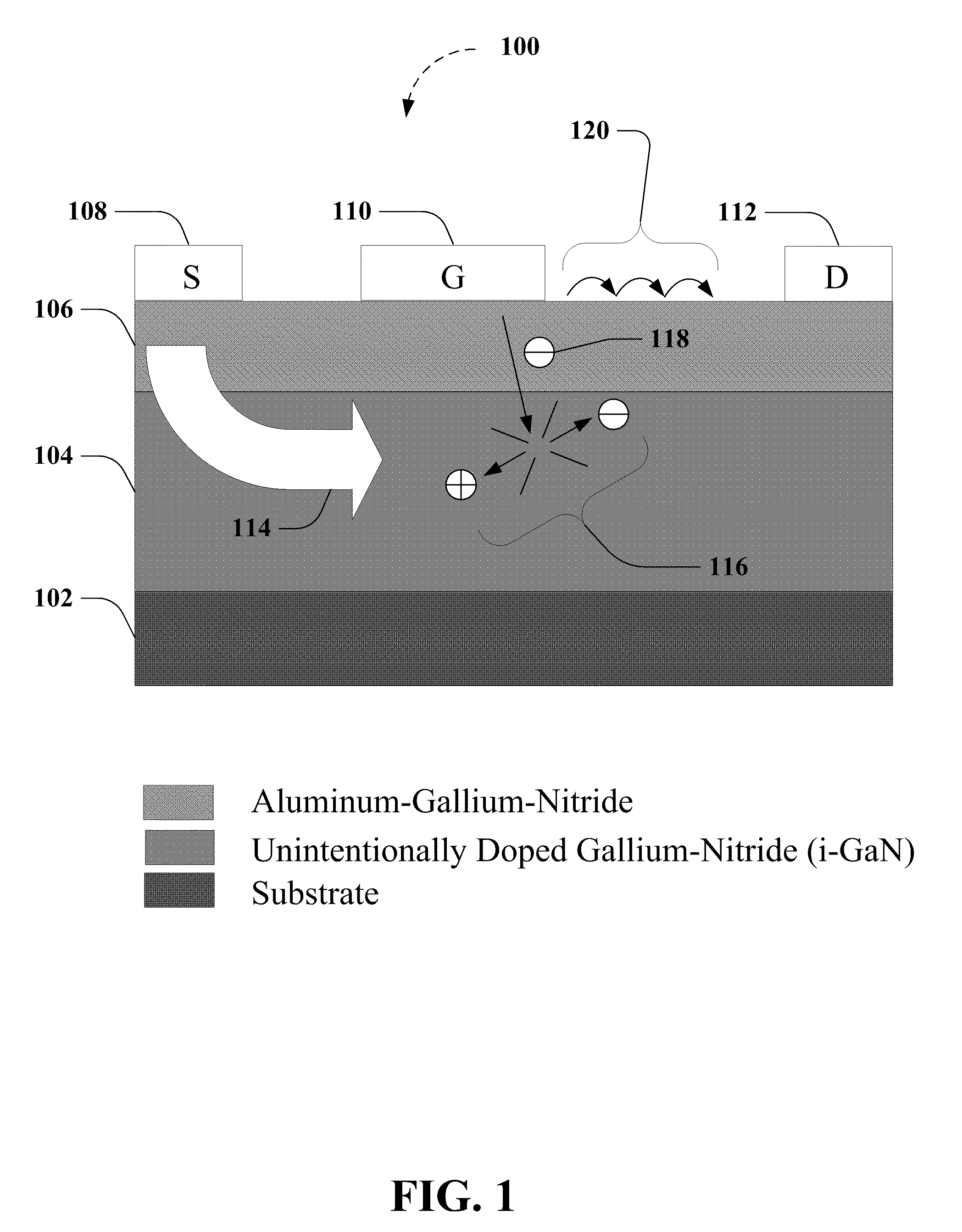
[0050]As described above, reported off-state breakdown voltage values for AlGaN / GaN HEMTs still remain significantly below the theoretical limit. It has been shown that the DIBL effect is significant even for micron gate length devices due to the unintentionally n-type background doping of the GaN buffer in state-of-the-art AlGaN / GaN HEMT devices.

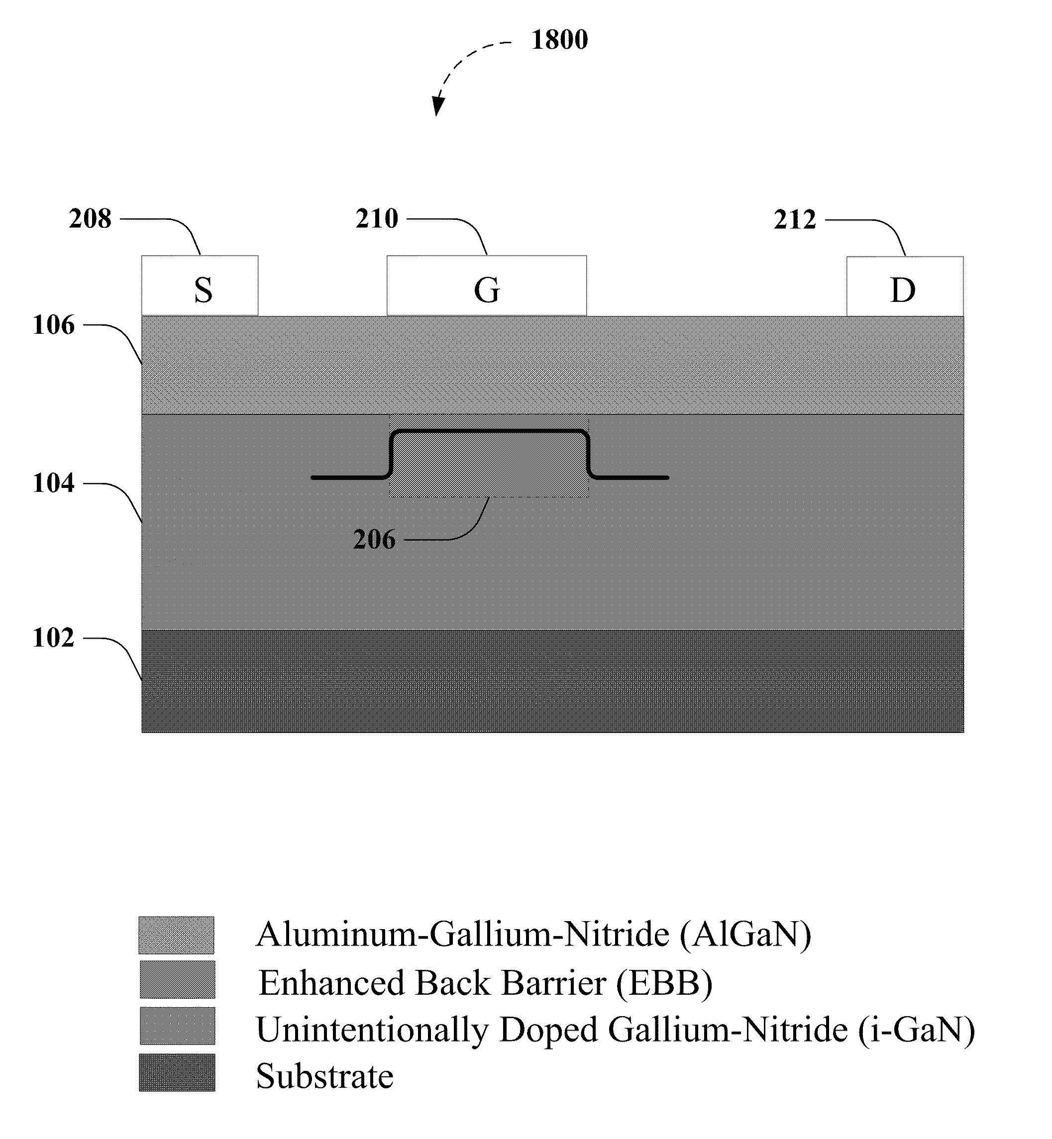
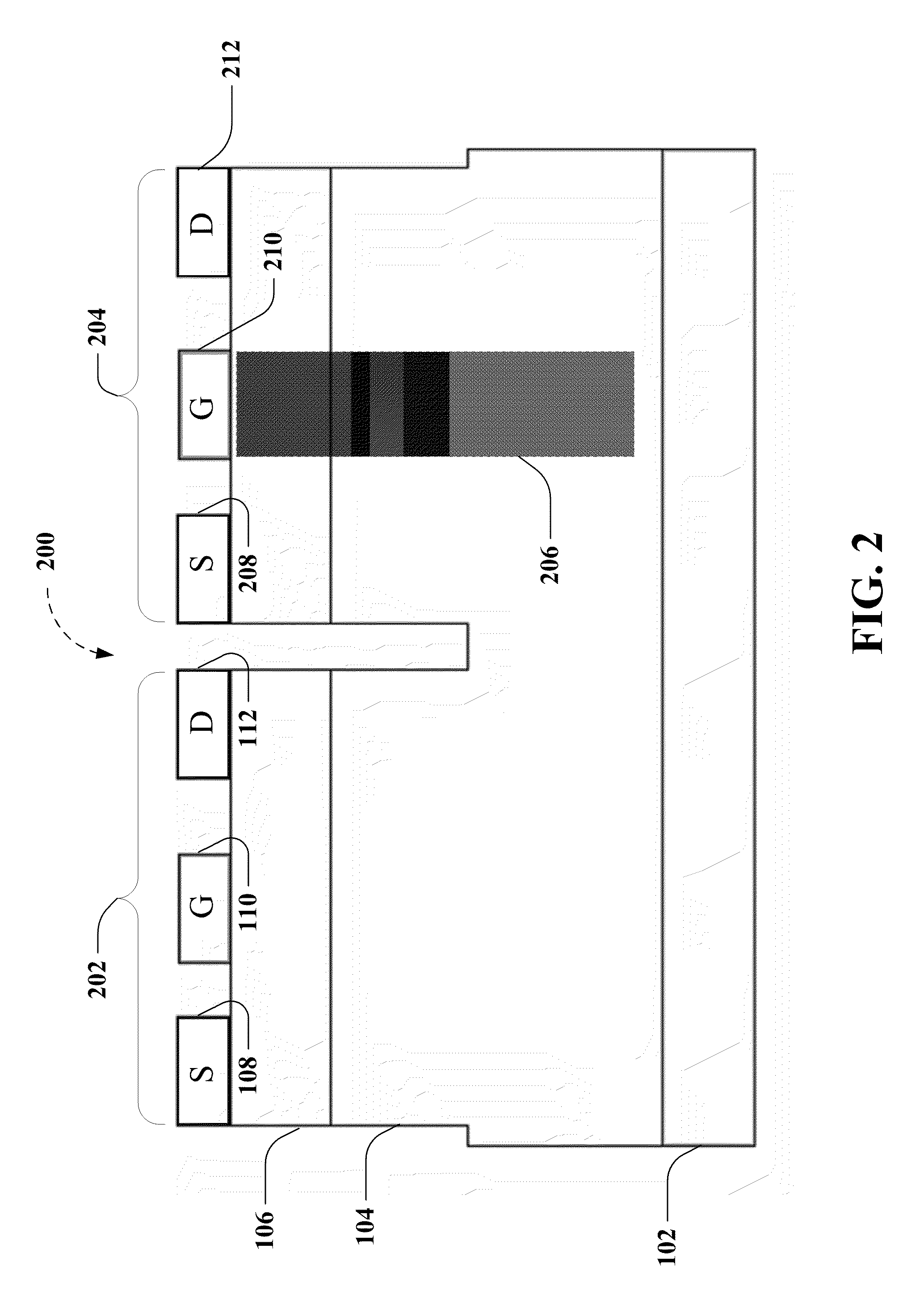
[0051]FIG. 1 depicts a schematic cross section view of a conventional AlGaN / GaN high electron mobility transistor, in which off-state breakdown mechanisms in AlGaN / GaN HEMTs are illustrated. AlGaN / GaN-HEMTs can typically be fabricated on a substrate 102 (e.g., sapphire, Silicon (Si), Silicon Carbide (SiC), etc.) b...


PUM


Abstract

Structures, devices and methods are provided for creating enhanced back barriers that improve the off-state breakdown and blocking characteristics in aluminum gallium nitride AlGaN/GaN high electron mobility transistors (HEMTs). In one aspect, selective fluorine ion implantation is employed when developing HEMTs to create the enhanced back barrier structures. By creating higher energy barriers at the back of the two-dimensional electron gas channel in the unintentionally doped GaN buffer, higher off-state breakdown voltage is advantageously provided and blocking capability is enhanced, while allowing for convenient and cost-effective post-epitaxial growth fabrication. Further non-limiting embodiments are provided that illustrate the advantages and flexibility of the disclosed structures.

Description

FIELD OF THE INVENTION[0001]This application claims priority to U.S. Provisional Patent Application Ser. No. 61 / 136,793, filed on Oct. 3, 2008, and entitled METHOD OF CREATING BACK BARRIER, AND ENHANCING THE OFF-STATE BREAKDOWN AND BLOCKING CAPABILITY IN AlGaN / GaN HEMT BY FLUORINE ION IMPLANTATION, the entirety of which is hereby incorporated by reference.FIELD OF THE INVENTION[0002]The subject disclosure is directed to field effect transistors and, more specifically, to structures, devices, and methods for creating a back barrier and enhancing off-state breakdown and blocking characteristics in Aluminum Gallium Nitride / Gallium Nitride (AlGaN / GaN) High Electron Mobility Transistors (HEMTs) by fluorine ion implantation.BACKGROUND OF THE INVENTION[0003]High Electron Mobility Transistors (HEMTs), also called heterostructure field-effect transistors (HFETs) or modulation-doped field-effect transistors (MODFETs), are field effect transistors typically incorporating a junction between two...

Claims


Application Information

Patent Timeline
IPC IPC(8): H01L29/778H01L21/335
CPCH01L29/2003H01L29/207H01L29/7788H01L29/7783H01L29/66462
Inventor CHEN, JINGWANG, MAOJUN
Owner THE HONG KONG UNIV OF SCI & TECH
Why Eureka
Try Eureka