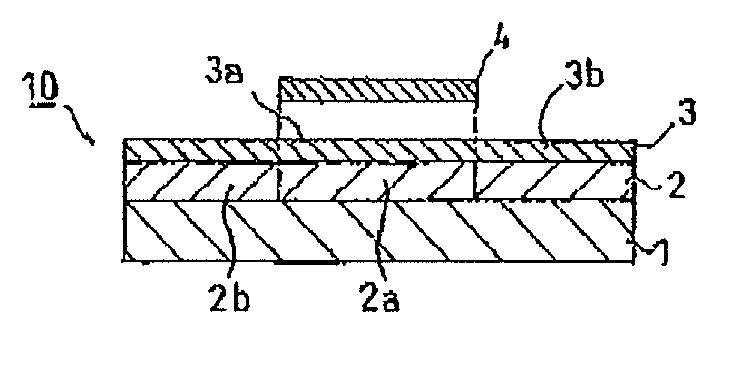
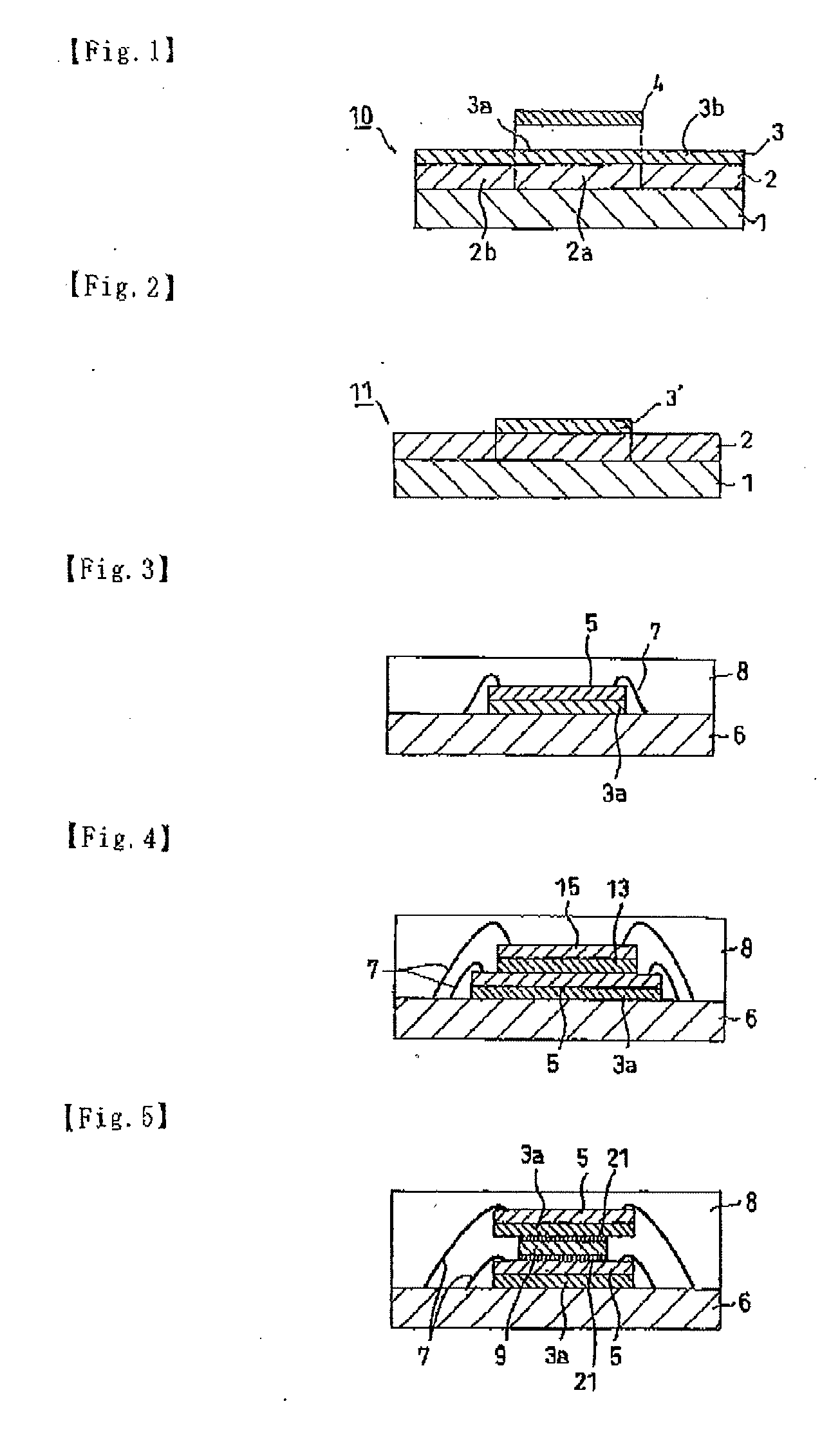
Dicing/die bonding film
- Summary
- Abstract
- Description
- Claims
- Application Information
AI Technical Summary
Benefits of technology
Problems solved by technology
Method used
Image

Examples
example 1
[0131]A solution of an adhesive composition having concentration 20% by weight was prepared by dissolving an isocyanate cross-linking agent (Coronate HX manufactured by Nippon Polyurethane Industry Co., Ltd) 3 parts by weight, an epoxy resin (EPIKOTE 1003 manufactured by Japan Epoxy Resins Co., Ltd.) 12 parts, a phenol resin (MILEX XLC-CC manufactured by Mitsui Chemicals, Inc.) 7 parts, and titanium oxide modified silicon dioxide (average particle size: 0.5 μm, ST-600 manufactured by TOKOYAMA Corp.) 20 parts as the inorganic filler materials to a polymer (Parakuron SN-710 manufactured by Negami Chemical Industrial Co., Ltd.) 100 parts by weight having butylacrylate as a main component into methylethylketone.
[0132]This solution of the adhesive composition was applied with a fountain coater onto a release treated film (a core material) consisting of a polyethylene terephthalate film (thickness 50 μm) on which a silicone releasing treatment was performed, and it was dried with a hot ai...
example 2
[0133]An acrylic pressure-sensitive adhesive was prepared in which 3 parts by weight of an isocyanate cross-linking agent (Coronate HX manufactured by Nippon Polyurethane Industry Co., Ltd) was added to an acrylic pressure-sensitive adhesive material 100 Parts by weight. Moreover, a die bond layer according to the present Example 2 was produced in the same manner as the above--described Example 1 except that an acrylic copolymer having 2-ethylhexyl acrylate 70 parts, n-butyl acrylate 25 parts, and acrylic acid 5 parts by weight as constituting monomers was compounded in the above-described acrylic pressure-sensitive adhesive and that the adhesive solution was prepared by dissolving silicon dioxide (average particle size 0.5 μm manufactured by Nippon Shokubai Co., Ltd.) 30 parts as the inorganic filler materials into methylethylketone so that the concentration become 20% by weight.
PUM
| Property | Measurement | Unit |
|---|---|---|
| Temperature | aaaaa | aaaaa |
| Length | aaaaa | aaaaa |
| Length | aaaaa | aaaaa |
Abstract
Description
Claims
Application Information
 - Generate Ideas
- Intellectual Property
- Life Sciences
- Materials
- Tech Scout
- Unparalleled Data Quality
- Higher Quality Content
- 60% Fewer Hallucinations
Browse by: Latest US Patents, China's latest patents, Technical Efficacy Thesaurus, Application Domain, Technology Topic, Popular Technical Reports.
© 2025 PatSnap. All rights reserved.Legal|Privacy policy|Modern Slavery Act Transparency Statement|Sitemap|About US| Contact US: help@patsnap.com