Specifically, any differences in the respective Coefficient of
Thermal Expansion (CTE) between the semiconductor and the
metal substrate can result in large “built-in” residual stresses that can have detrimental effects on the semiconductor device performance.
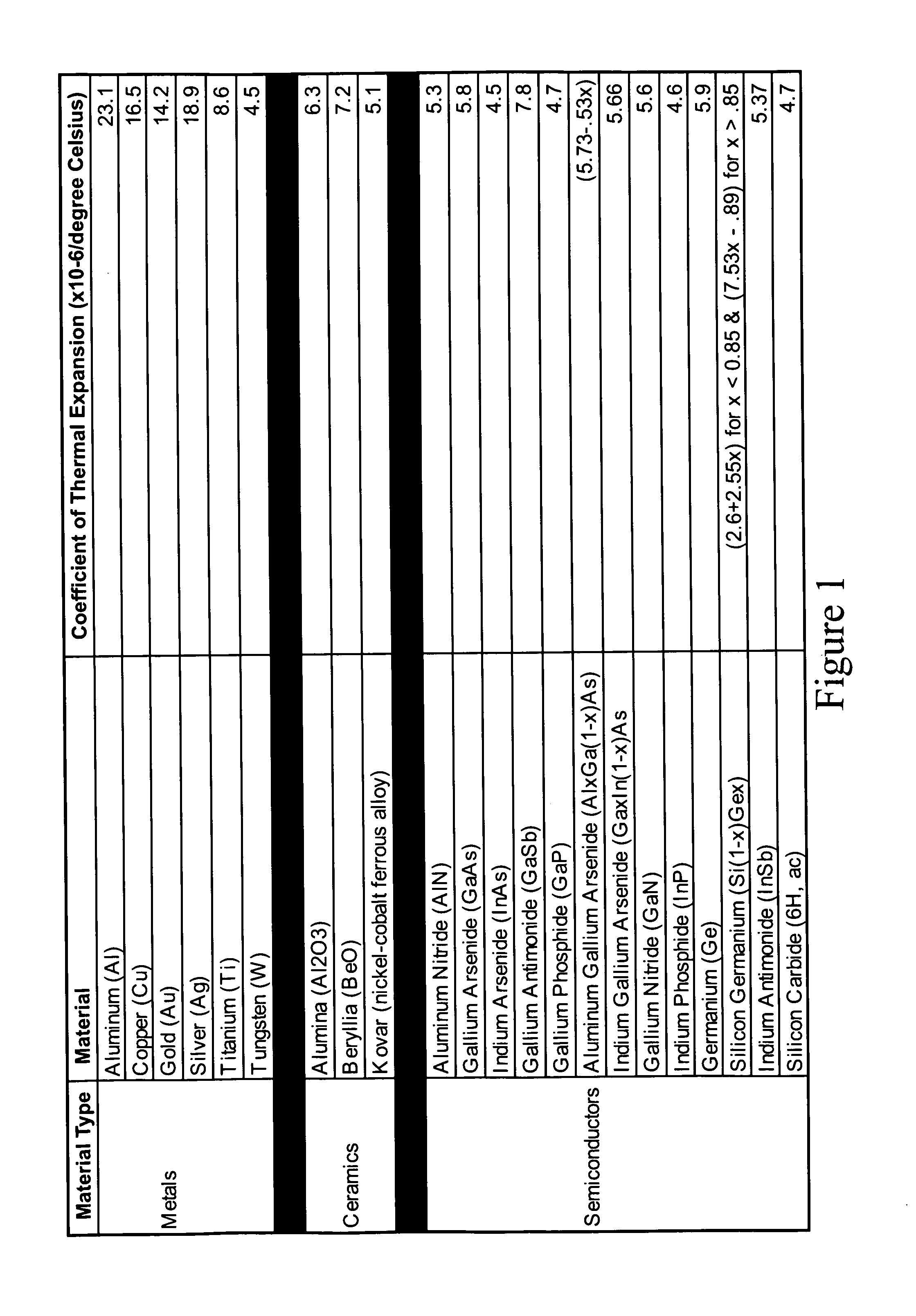
Metals usually have relatively large coefficients of
thermal expansion, whereas semiconductors have comparatively lower coefficients of
thermal expansion, and therefore, the differing thermal expansion coefficients of the materials in this
system, combined with the elevated temperatures required to perform the
soldering process, can result in large built-in stresses between the mated substrates once they are cooled to
room temperature.
Additionally, most semiconductor devices heat up very significantly during operation and can result in thermal stresses and strains to develop between the semiconductor device and the
metal substrate it is mounted to.
Specifically, this operational heating combined with the differing coefficients of thermal expansion results in a thermal stress and strain on the semiconductor devices.
These built-in stresses frequently result in many negative consequences for the performance of semiconductor device(s).
Furthermore, large built-in stresses have been known to appreciably lower the reliability of semiconductor devices.
For example, most semiconductor devices heat-up due to the power dissipated during operation thereby resulting in a
thermal strain to develop between the mated materials.
Under some circumstances, this
thermal strain can become sufficiently large so as to result in the fracture of the semiconductor substrate, thereby resulting in an inoperable semiconductor device(s).
Additionally, a sufficiently large
thermal strain between a joined semiconductor and
metal substrate can result in the substrates breaking apart due to a failure at the interface.
Moreover, even if the thermal strain is not sufficiently large to cause fracture in one operational cycle, fracture can still result after many operational cycles (e.g., power on for some period of time with a
resultant increase in heating and thermal
stain, followed by a period of time with the power off and a decrease in heating and thermal strain, followed by a period of time with power on again with a
resultant increase in heating and thermal strain, etc.), due to fatigue effects in the semiconductor substrate over multiple cycles of operation.
Even in cases where fracture due to fatigue does not occur, the additional strain will lower the reliability of the
solid-state semiconductor devices.
For example, a
laser diode that is under a strain due to packaging or mounting stresses will have its bandgap in the semiconductor modified and this change in the bandgap may result in increased currents at certain locations in the device that, if sufficiently large, will overstress the material and eventually cause it to fail.
In the case of light emitting devices the additional strain will result in undesirable
wavelength shifts, thereby decreasing the performance of the device.
Additionally, it is known that the thermal and mechanical stresses between semiconductor substrates mounted onto metal substrates can cause the solders used to join the metal and semiconductors substrates to re-flow from the interface to other areas of the device and / or
package, which can result in a number of problems, such as the
electrical shorting of the device.
In some instances, this solder may re-flow to locations that cause an
electrical shorting between parts of the device meant to be electronically isolated thereby resulting in
catastrophic failure of the device.
Solder re-flow may also result in the
solder material encroaching and obstructing into sensitive locations of the device.
Alternatively, or in addition to these phenomena, the solder layer(s) used for joining metal to semiconductor substrates can re-flow away from the areas where
electrical current is flowing and
voltage potential is applied, thereby resulting in an open circuit condition, as well as other serious and negative effects on the semiconductor device(s).
If the solder re-flows from the interface between the metal and semiconductor substrates, the result could be the creation of voids at certain locations and an accompanying increase in the electrical resistance across the metal to semiconductor interface in locations where the solder is no longer present.
Moreover, in the locations where the solder has moved away from the interface, thereby forming voids in the electrical continuity at the metal to semiconductor junction, the re-flow process, if left to continue, can eventually result in an open-circuit condition of the device.
Furthermore, in the locations where the current is concentrated, the temperature of the interface will rise, thereby causing more solder to re-flow and consequently reinforcing the process to continue or even accelerate it, with the eventual result that the semiconductor device(s) fails to operate.
As a result, the temperature of the semiconductor device(s) will rise since the heat cannot be transferred as effectively away from the semiconductor substrate.
Consequently, a
positive feedback process is established whereby the semiconductor device and substrate heating reinforces the solder migration, which causes additional temperature rise in the semiconductor, with the eventuality that the semiconductor fails to operate.
Even for semiconductor devices where the result is not
catastrophic failure, overheating caused by solder re-flow can have very serious consequences for the reliability of the semiconductor device(s).
Therefore, it can be seen that as the temperature rises, the rate of failure increases exponentially.
Therefore, for some devices, even relatively small temperature increases (e.g., a few degrees Celsius), can result in a very large decrease in device reliability.
Therefore, any phenomena resulting in even a slight over-temperature of the semiconductor devices will have significant and negative effects on the semiconductor device reliability.
Even if other materials, such as adhesives, epoxies, glues, etc., are used to join or attach a semiconductor substrate to a
metal substrate, there can be appreciable and undesired stresses in the semiconductor substrates partially or totally as a result of the large thermal expansion coefficient mis-match between most
metallic materials and semiconductors.
Additionally, adhesives tend to shrink when they cure, which also can lead to significant stresses and strains in the semiconductor substrate and the associated increase in problems with reliability and failures.


