Method of reducing non-uniformities during chemical mechanical polishing of microstructure devices by using cmp pads in a glazed mode

a microstructure device and cmp pad technology, applied in the direction of abrasive surface conditioning devices, manufacturing tools, lapping machines, etc., can solve the problems of reducing the uniformity of the surface of the microstructure device, the inability to efficiently etch the anisotropic etch technique, etc., to achieve enhanced process control, reduce the surface roughness, and reduce the effect of down for

Inactive Publication Date: 2010-05-06
ADVANCED MICRO DEVICES INC
View PDF5 Cites 4 Cited by
  • Summary
  • Abstract
  • Description
  • Claims
  • Application Information

AI Technical Summary

Benefits of technology

[0013]Generally, the present invention relates to techniques for planarizing or generally removing material from a layer system of a microstructure device at reduced down forces during the polishing process, while nevertheless providing a desired removal rate in combination with enhanced process control with respect to uniformity of the resulting surface topography. For this purpose, the polishing process may be performed on the basis of a polishing pad having a state of reduced surface roughness, which may thus contribute to enhanced overall process uniformity in combination with highly chemically reactive slurry materials. The reduced surface roughness of the polishing pad may be established by controlling the degree of conditioning of the polishing pad such that a moderately high degree of glazing may intentionally be maintained so as to adapt the mechanical removal component for the benefit of enhanced surface topography. Consequently, sophisticated layer stacks, such as metallization systems including low-k dielectric materials in combination with a soft metal, such as copper, may be efficiently planarized on the basis of reduced down forces, while also maintaining the overall removal rate at a desired high value due to the usage of a chemically reactive slurry material. On the other hand, due to the increased degree of glazing of the polishing pad, which may be maintained at least at a final phase of the polishing process, i.e., during the exposure of a dielectric material and a corresponding overpolish time, which may be required so as to reliably electrically insulate respective metal regions from each other, the reduced surface roughness of the glazed polishing pad may provide a corresponding reduction and thus adaptation of the overall removal rate. Hence, in this critical phase of the polishing process, metal may still be removed from dielectric surface portions to be cleared, while undue dishing, i.e., undue recessing metal in the metal regions, may be reduced, which may translate into enhanced performance of the corresponding metal regions since generally an increased cross-sectional area may be maintained.

Problems solved by technology

Although copper and alloys thereof exhibit superior characteristics compared to aluminum in terms of conductivity and resistance against electromigration, many problems are involved in processing copper-based materials in a semiconductor facility, one of which resides in the fact that copper may not be very efficiently deposited in large amounts with well-established deposition techniques such as chemical vapor deposition (CVD) and sputter deposition.
Moreover, copper may not be efficiently patterned by conventional anisotropic etch techniques.
Completely removing the conductive material from a substrate having a diameter of 200 or 300 mm is, however, a challenging task and usually leads to a certain amount of dishing and erosion of the metallization structures.
In particular, if a plurality of sophisticated metallization layers are stacked so as to form the metallization system of an advanced integrated circuit, typically, highly sensitive dielectric materials having a reduced permittivity, and thus also a significantly reduced mechanical stability, may result in a highly sensitive layer stack, which may require significantly reduced down forces during the polishing process so as to not unduly cause damage in the metallization system.
Upon contact of the polishing pad and the surface to be polished, abrasive particles, which may be contained in the slurry material, and corresponding polish byproducts may increasingly accumulate in the pores of the polishing pad, thereby reducing the capability of efficiently distributing slurry.
Furthermore, the accumulation of particles and polishing byproducts may increasingly result in a “hardening” of the surface, which is typically referred to as glazing, which may result in a significant drop of removal rate due to a reduced degree of surface roughness of the polishing pad in combination with a reduced capability of distributing the slurry material.

Method used


Image

  • Method of reducing non-uniformities during chemical mechanical polishing of microstructure devices by using cmp pads in a glazed mode
  • Method of reducing non-uniformities during chemical mechanical polishing of microstructure devices by using cmp pads in a glazed mode
  • Method of reducing non-uniformities during chemical mechanical polishing of microstructure devices by using cmp pads in a glazed mode

Examples


Embodiment Construction

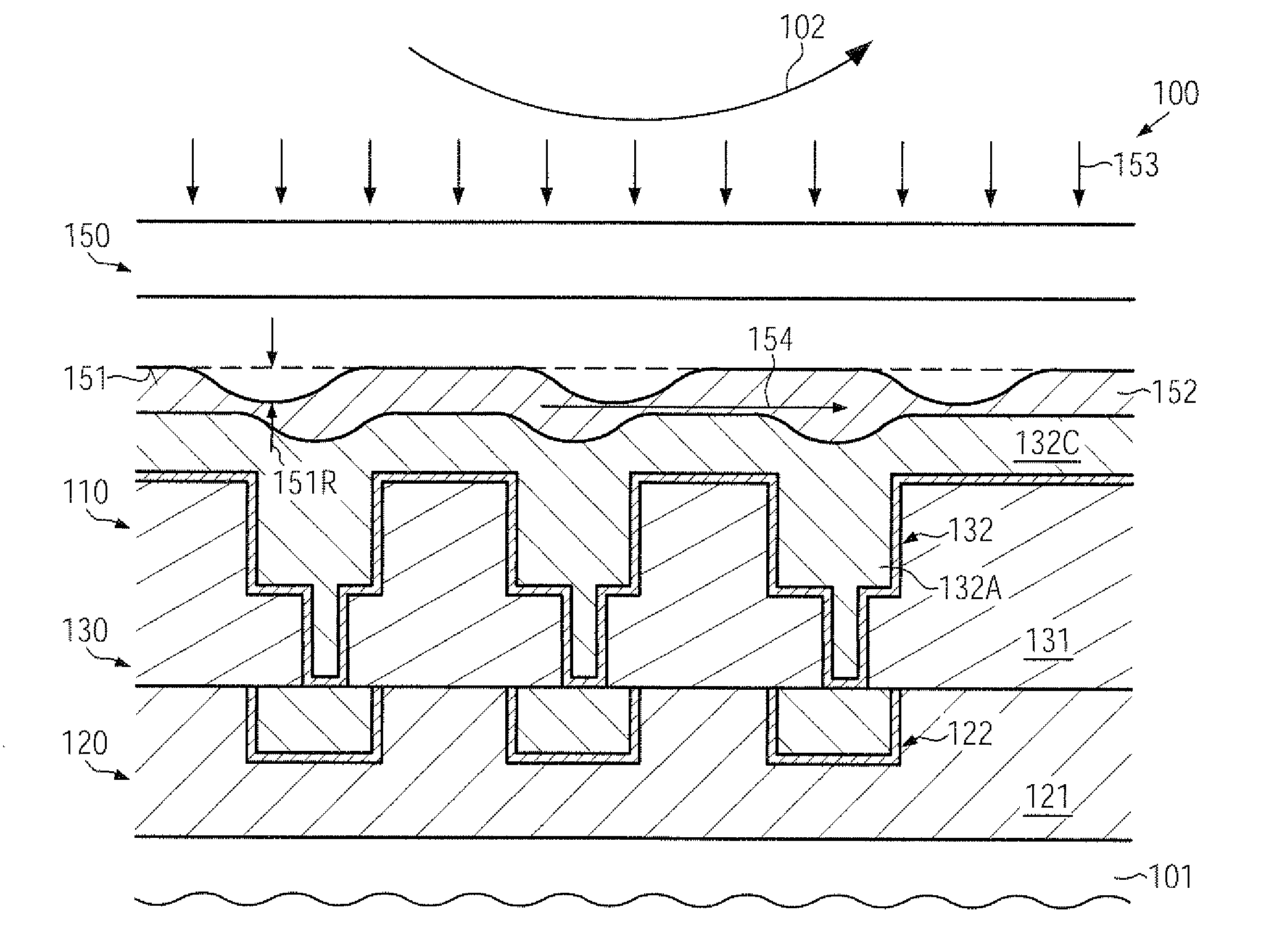
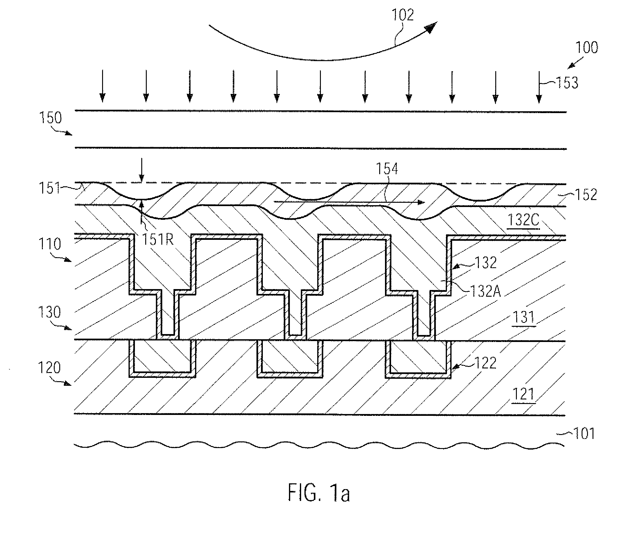
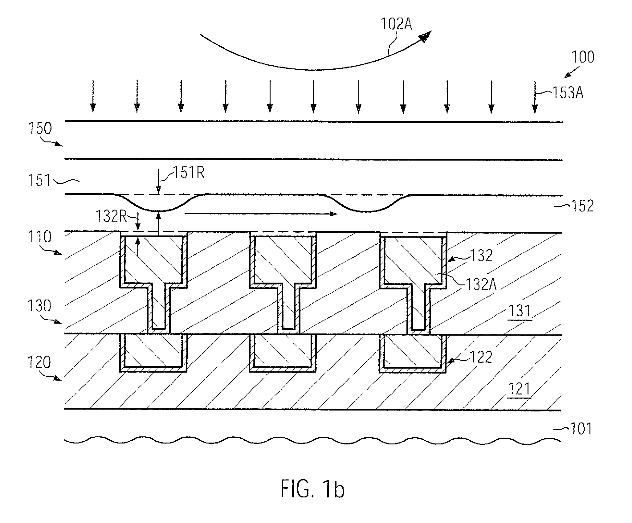
[0023]Various illustrative embodiments of the invention are described below. In the interest of clarity, not all features of an actual implementation are described in this specification. It will of course be appreciated that in the development of any such actual embodiment, numerous implementation-specific decisions must be made to achieve the developers' specific goals, such as compliance with system-related and business-related constraints, which will vary from one implementation to another. Moreover, it will be appreciated that such a development effort might be complex and time-consuming, but would nevertheless be a routine undertaking for those of ordinary skill in the art having the benefit of this disclosure.

[0024]The present subject matter will now be described with reference to the attached figures. Various structures, systems and devices are schematically depicted in the drawings for purposes of explanation only and so as to not obscure the present disclosure with details ...


PUM

PropertyMeasurementUnit
diameteraaaaaaaaaa
diameteraaaaaaaaaa
dielectric constantaaaaaaaaaa

Abstract

In sophisticated CMP recipes, the material removal may be accomplished on the basis of a chemically reactive slurry material and a reduced down force, wherein the surface topography of a finally obtained material layer may be enhanced by using, at least in a final phase, a glazed state of the polishing pad.

Description

BACKGROUND OF THE INVENTION[0001]1. Field of the Invention[0002]The present disclosure generally relates to the field of fabricating microstructure devices, such as integrated circuits, and, more particularly, to the planarization of a metallization layer and / or the removal of excess metal from a dielectric layer.[0003]2. Description of the Related Art[0004]In manufacturing microstructures, such as integrated circuits, various material layers are deposited on a substrate and are patterned by lithography, such as photolithography, and etch processes and the like to provide a large number of individual features, such as circuit elements in the form of transistors, capacitors, resistors, interconnect structures and the like. Due to the continuous reduction of feature sizes of the individual structure elements, sophisticated lithography and etch techniques have been developed that allow the resolution of critical dimensions, i.e., of minimum feature sizes, well beyond the wavelength of ...

Claims


Application Information

Patent Timeline
Patent Type & Authority Applications(United States)
IPC IPC(8): H01L21/306B24B1/00
CPCB24B37/042B24B49/00B24B53/017H01L21/3212H01L21/7684
Inventor MARXSEN, GERDHEINRICH, JENSSCHLOTT, JANA
Owner ADVANCED MICRO DEVICES INC
Why Eureka
Try Eureka