
Solar cells

a photovoltaic device and organic technology, applied in the field of thin film crystalline organic photovoltaic devices, can solve the problems of low photovoltaic performance, low external quantum efficiency, and inability to provide power to circuits, devices or equipment, etc., and achieve high external quantum efficiency and improve photovoltaic performance.

Active Publication Date: 2010-05-13
THE TRUSTEES FOR PRINCETON UNIV
View PDF22 Cites 32 Cited by
  • Summary
  • Abstract
  • Description
  • Claims
  • Application Information

AI Technical Summary

Benefits of technology

[0029]It is an object of the present invention to provide an organic PV device with improved photovoltaic performance. To this end, the invention provides an organic PV device capable of operating with a high external quantum efficiency.

Problems solved by technology

As a general rule, a photovoltaic cell provides power to a circuit, device or equipment, but does not provide a signal or current to control detection circuitry, or the output of information from the detection circuitry.
In contrast, a photodetector or photoconductor provides a signal or current to control detection circuitry, or the output of information from the detection circuitry but does not provide power to the circuitry, device or equipment.
However, efficient crystalline-based devices, especially of large surface area, are difficult and expensive to produce due to the problems inherent in producing large crystals without significant efficiency-degrading defects.
On the other hand, high efficiency amorphous silicon devices still suffer from problems with stability.
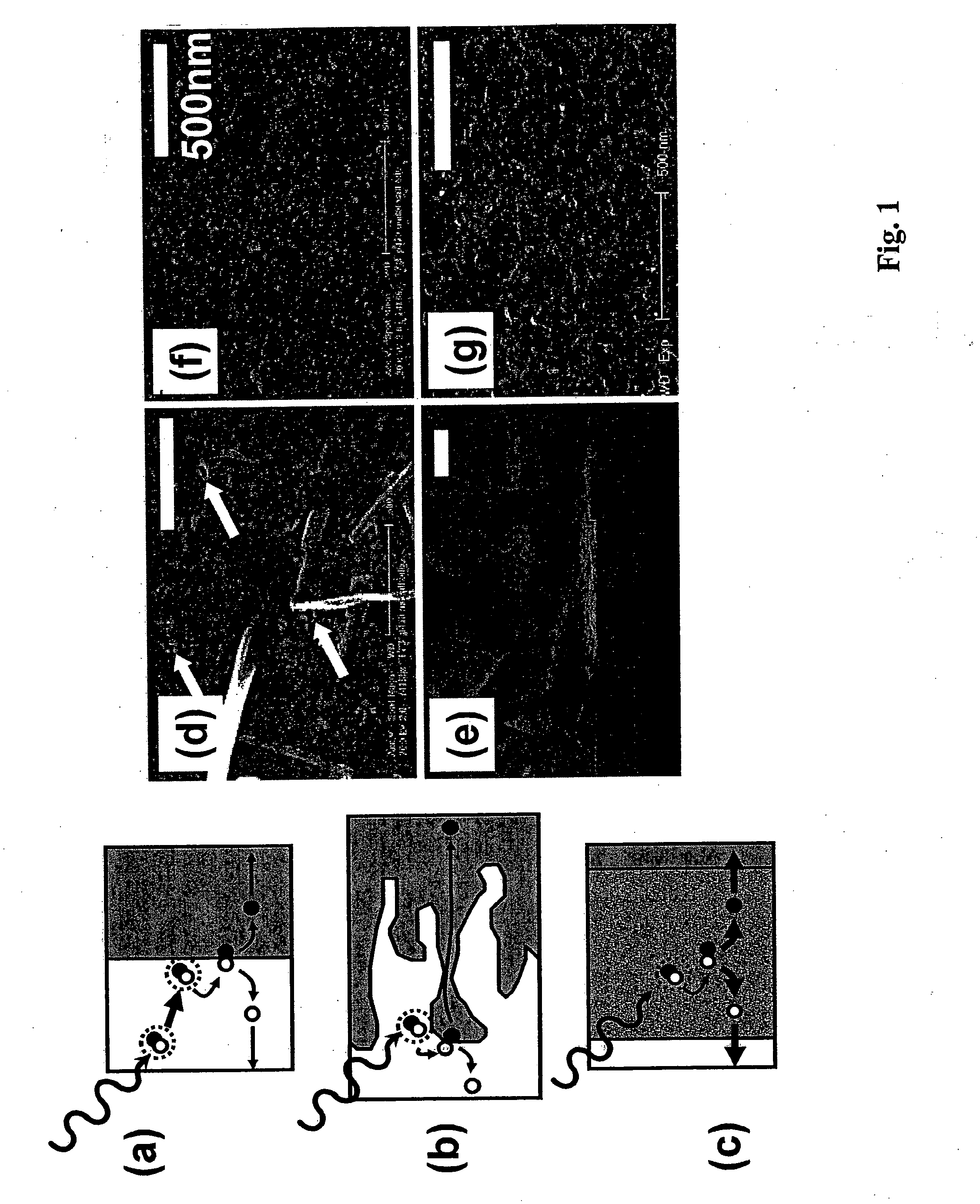
Such a process can be induced by the built-in electric field, but the efficiency at the electric fields typically found in organic devices (F˜106 V / cm) is low.
However, some organic PV devices typically have relatively low external quantum efficiency, being on the order of 1% or less.
To date none of these proposals has led to a significant improvement in overall cell performance, particularly at high illumination intensities.
In this process energy is lost which will result in a lower efficiency for the device.

Method used


Image

  • Solar cells
  • Solar cells
  • Solar cells

Examples


example 1

[0096]The PV cells were deposited on glass substrates pre-coated with a 1500 Å thick, transparent, conducting indium-tin-oxide (ITO) anode (sheet resistance 40 Ω / □). The substrates were cleaned immediately prior to transferring them into the vacuum system for film deposition. The organic materials were commercially obtained and purified prior to deposition using thermal gradient sublimation. The photoactive materials used were copper phthalocyanine (CuPc) and 3,4,9,10-perylenetetracarboxylic bis-benzimidazole (PTCBI), and bathocuproine (BCP) was used as a contact buffer layer. The organic layers were grown by high vacuum thermal evaporation (base pressure 10−7-10−6 Torr) from a tungsten boat onto a room-temperature substrate. This was followed by the deposition of the metal cathode through a shadow mask, resulting in contact diameters of 0.3 mm and 1 mm.

[0097]After fabrication, the cells were transferred to a vacuum chamber held at 30 m Ton with a heating stage, electrical probes an...

example 2

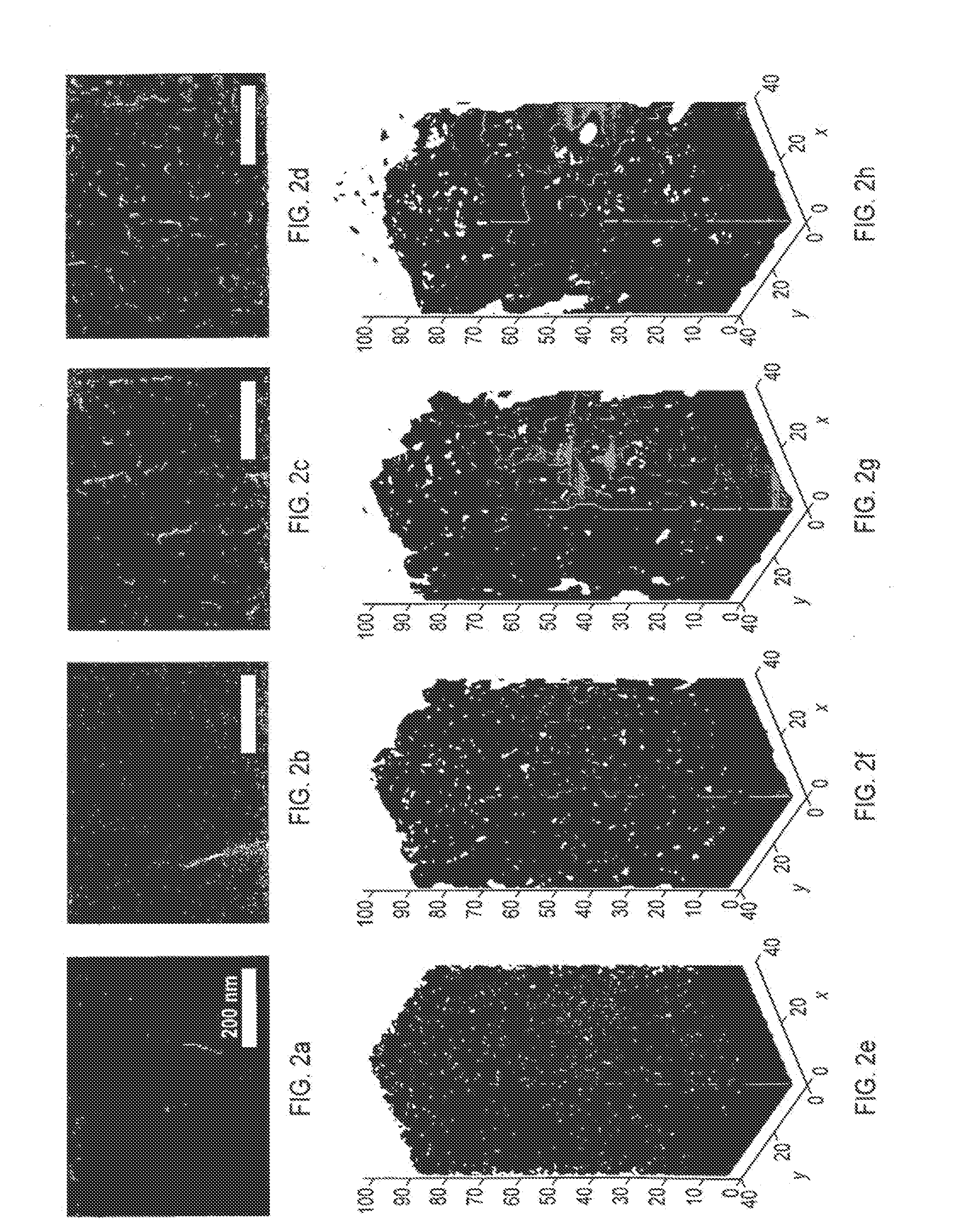
[0100]FIG. 2 contains SEM images of cross-sections of the layer structure: ITO / 5000 Å CuPc:PTCBI (4:1) / 1000 Å Ag are shown for (a) an as-grown film, and for films annealed for 15 min at (b) TA1=450K, (c) TA1=500K, and (d) TA1=550K. The images show phase segregated domains, alternatively rich in CuPc and PTCBI, the cross-sections revealing domains whose size increases with increasing annealing temperature. At 550K, domain sizes of ˜20 nm are observed.

example 3

[0101]Domain sizes of 20 nm are confirmed by the X-Ray diffraction data shown in FIG. 3. Upon annealing, diffraction peaks corresponding to the orthorhombic α-CuPc phase emerge, and the broad amorphous background signal between 2Θ=2.5° and 12.5° is reduced. The large width of the peaks suggests limited crystalline domain size. For the film annealed at 550K, using the FWHM (full width half maximum) of the peaks at 2Θ=6.7° and 2Θ=12.2° , we calculate a domain size of (12±1)nm, which is consistent with the observations in FIG. 2. This represents a lower limit to the domain size, as the diffraction peaks are also broadened by molecular disorder and large strains associated with the growth of domains within an amorphous matrix. Additional potential contribution to the peak width is residual “doping” of the CuPc and PTCBI-rich phases with PTCBI and CuPc, respectively.


PUM


Abstract

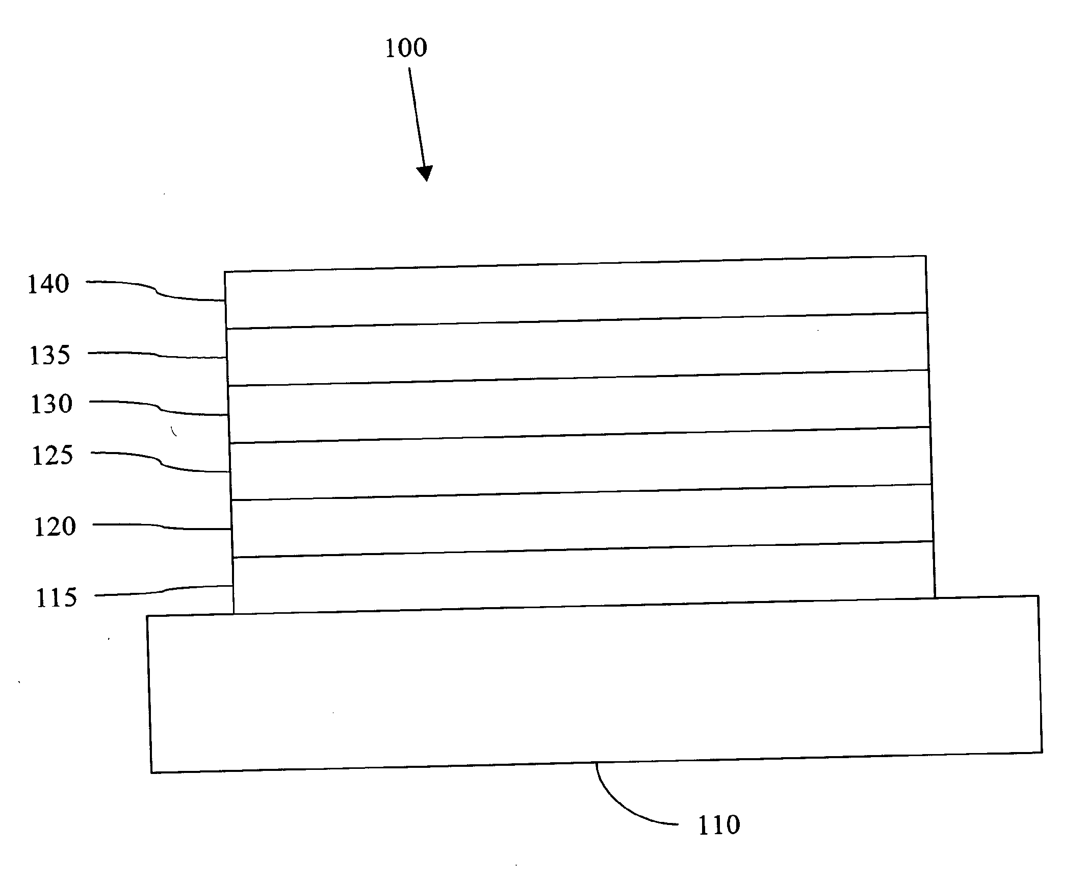
Organic photosensitive optoelectronic devices are disclosed. The devises are thin-film crystalline organic optoelectronic devices capable of generating a voltage when exposed to light, and prepared by a method including the steps of: depositing a first organic layer over a first electrode; depositing a second organic layer over the first organic layer; depositing a confining layer over the second organic layer to form a stack; annealing the stack; and finally depositing a second electrode over the second organic layer.

Description

FIELD OF INVENTION[0001]The present invention generally relates to organic photosensitive optoelectronic devices. More specifically, it is directed to thin-film crystalline organic photovoltaic devices, e.g., organic solar cells prepared by annealing.BACKGROUND OF THE INVENTION[0002]Optoelectronic devices rely on the optical and electronic properties of materials to either produce or detect electromagnetic radiation electronically or to generate electricity from ambient electromagnetic radiation.[0003]Photosensitive optoelectronic devices convert electromagnetic radiation into electricity. Solar cells, also called photovoltaic (PV) devices, are a type of photosensitive optoelectronic device that is specifically used to generate electrical power. PV devices, which may generate electrical energy from light sources other than sunlight, can be used to drive power consuming loads to provide, for example, lighting, heating, or to power electronic circuitry or devices such as calculators, ...

Claims


Application Information

Patent Timeline
Patent Type & Authority Applications(United States)
IPC IPC(8): H01L31/042H01L31/00H10K99/00
CPCH01L51/0026H01L51/0053H01L51/0078H01L51/4246H01L51/4253Y02E10/549H10K71/40H10K85/621H10K85/311H10K30/30H10K30/50H10K30/211
Inventor PEUMANS, PETERUCHIDA, SOICHIFORREST, STEPHEN R.
Owner THE TRUSTEES FOR PRINCETON UNIV
Learn More