Optical module

Inactive Publication Date: 2010-06-24
HITACHI LTD
View PDF1 Cites 34 Cited by
  • Summary
  • Abstract
  • Description
  • Claims
  • Application Information

AI Technical Summary

Benefits of technology

[0018]According to the present invention a laser beam high in both beam parallelism and beam-condensability can be attained by integrated light emitting devices, thus making it possible to simplify the optical system w

Problems solved by technology

In the conventional lens-semiconductor light emitting device integral combination, a limit is encountered in both alignment between light emitting devices and optical parts and also in the light focusing performance of micro lenses, and in coupling with an optical fiber for optical communication it has been difficult to obtain low coupling loss of 1 dB or less (20% or less).
However, in the conventional optical communication using laser beam as a signal carrier, a coupling loss of 1 dB or so does not arise a serious problem insofar as the lig

Method used


Image

  • Optical module
  • Optical module
  • Optical module

Examples


Example

First Embodiment

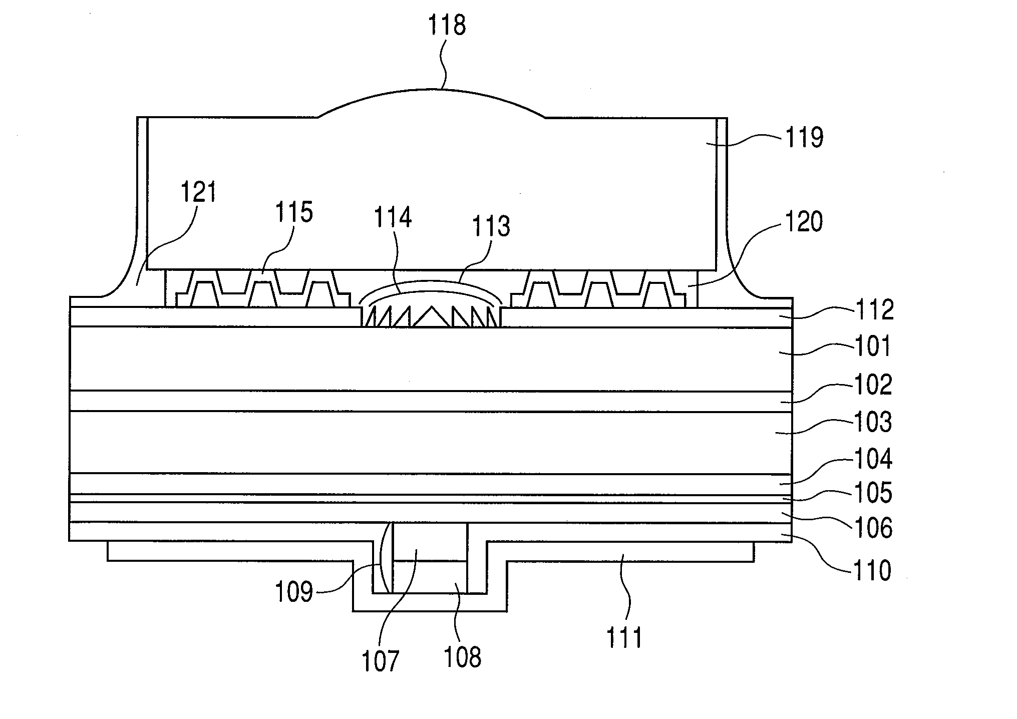
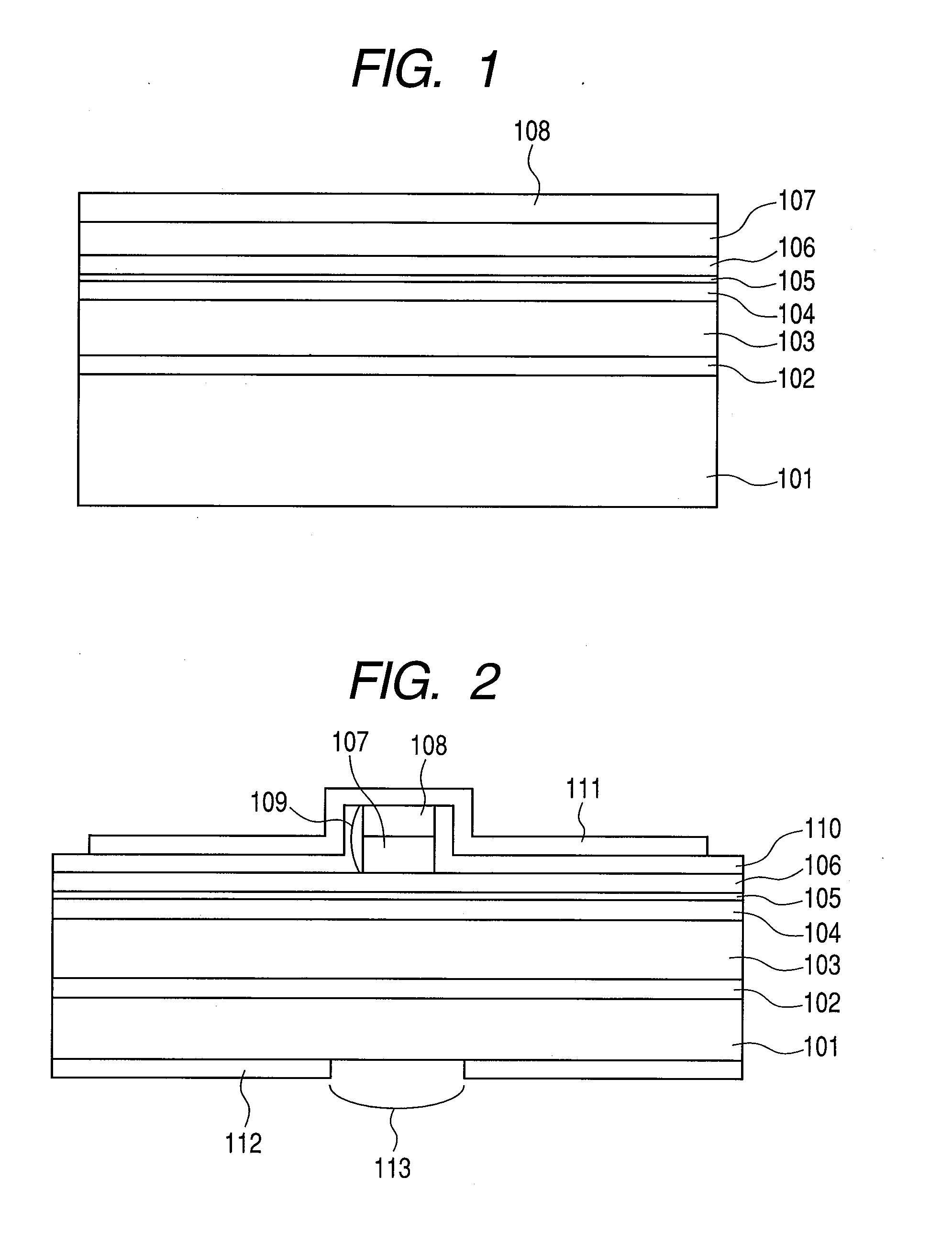
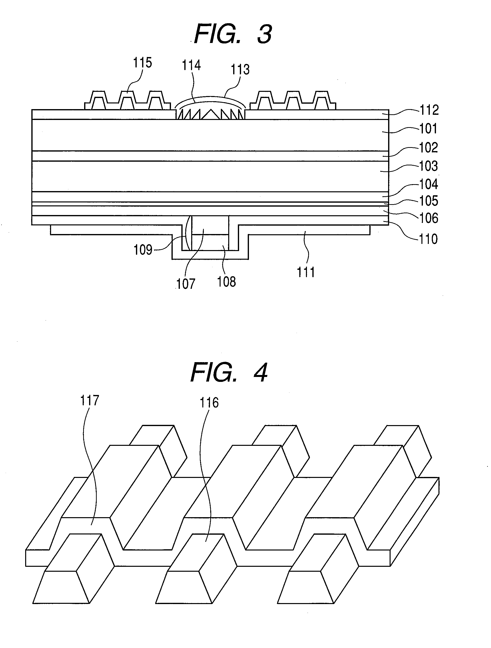
[0039]A first embodiment of the present invention will be described below in accordance with a device fabricating procedure. In this first embodiment, the semiconductor light emitting device is constructed as an AlGaInAs-based surface emitting type semiconductor laser with a wavelength of 1300 nm.

[0040]First, such single-crystal multilayers as shown in FIG. 1 are formed on an n-InP substrate 101 by metal organic chemical vapor deposition. More specifically, an n-InP buffer layer 102 and an n-type Bragg reflector 103 having a ¼ thick wavelength, which lattice-matches InP, are formed first. The n-type Bragg reflector 103 is constituted by a laminated film of n-InGaAs and n-InAlAs and has a reflectance of 99.8%. Subsequently, an n-InGaAlAs lower SCH (Separate Confinement Heterostructure) layer 104 lattice-matched with InP, a strained quantum well active layer 105 composed of an InGaAlAs strained barrier layer (band gap 1.32 eV, barrier layer thickness 8 nm) and an InGaA...

Example

[0049]A second embodiment of the present invention will now be described in accordance with a device fabrication procedure in which a semiconductor light emitting device is constituted as an AlGaInAs semiconductor laser with a wavelength of 1300 nm. First, such single-crystal multilayers as shown in FIG. 7 are formed on an n-InP substrate 101 by metal organic chemical vapor deposition. In forming the single crystal multilayer film, there first is formed a Bragg reflector 202 having an optical length of ¼ thick wavelength, which lattice-matches InP. The Bragg reflector 202 is constituted by a laminated film of n-InGaAs an n-InAlAs and has a reflectance of 70%. Subsequently, an n-InP lower cladding layer 203, a strained quantum well active layer 204 composed of an InGaAlAs strained barrier layer (band gap 132 eV, barrier layer thickness 8 nm) and an InGaAlAs strained quantum well layer (band gap 0.87 eV, well layer thickness 6 nm), a p-InP upper cladding layer 205, and a p-InGaAs cont...

Example

Third Embodiment

[0057]As a third embodiment of the present invention there is shown an example in which, instead of the plated spring, a foamed resin is used in the bonding portion between InP substrate and glass substrate. In this embodiment, the fabrication of light emitting devices on an InP substrate 101 is performed in the same way as in the second embodiment. Next, foamed silicone 301 is applied at a thickness of about 10 μm to the back surface of the substrate 101 and is allowed to foam and cure. Then, the foamed silicone 301 is subjected to photolithography so as to remain at only a portion exclusive of the portion of light emitting devices and lenses, affording the structure of FIG. 10. Under the foaming action, the foamed silicone after curing has a thickness of about 20 μm, still possessing a spongy flexibility permitting adjustment of the spacing between two wafers.

[0058]Next, using silicone-gel 120, a micro lens array 119 having micro lenses is bonded to the position co...


PUM


Abstract

An optical module comprising a laser device adapted to emit a laser beam from a convex surface and including a horizontal resonator surface-emitting structure provided with a first lens through which an optical axis of the laser beam passes, and a second lens through which the laser beam having passed through the first lens passes, a surface opposed to the second lens-provided surface and the surface provided with the first lens being bonded together through a first adhesive transparent to the laser beam.

Description

CLAIM OF PRIORITY[0001]The present application claims priority from Japanese patent application JP 2008-324917 filed on Dec. 22, 2008, the content of which is hereby incorporated by reference into this application.FIELD OF THE INVENTION[0002]The present invention relates to an optical module having a lens-integrated semiconductor laser device.BACKGROUND OF THE INVENTION[0003]In connection with a lens-integrated composite optical device there have been known such conventional techniques as those described in JP-A-2002-26452, JP-A-2004-311861, and JP-T-2001-519601.[0004]The structure described in JP-A-2002-26452 is shown in FIG. 17. This structure is provided with a VCSEL array substrate with vertical cavity surface emitting lasers arranged thereon and a lens array substrate integral with the VCSEL array substrate, the lens array substrate having lenses formed at positions corresponding to the surface emitting lasers. The VCSEL array substrate and the lens array substrate are fabricat...

Claims


Application Information

Patent Timeline
IPC IPC(8): H01S5/42H01S5/183H01S5/20H01S5/026G02B6/42H01S5/12
CPCG02B6/4206G02B6/4214H01S5/005H01S5/026H01S5/32341H01S5/028H01S5/1085H01S5/12H01S5/187H01S5/0267
Inventor NAKATSUKA, SHINICHIMATSUOKA, YASUNOBU
Owner HITACHI LTD
Why Eureka
Try Eureka