Manufacturing method for a solid-state image sensor

Active Publication Date: 2010-08-12
CANON KK
View PDF33 Cites 30 Cited by
  • Summary
  • Abstract
  • Description
  • Claims
  • Application Information

AI Technical Summary

Benefits of technology

[0014]It is therefore an object of the present invention to provide more specific manufacturing conditions with respect to RTA techniques in a manufacturing method for a solid-state image sensor, thus enablin

Problems solved by technology

If enhanced diffusion causes a high-concentration surface region to diffuse toward the interior of the semiconductor substrate, the concentration of the charge storage region will suddenly drop, causing an extreme decrease in the ability to store electrons or holes.
In solid-state image sensors, such a decrease in ability causes the saturation characteristics to degrade.
Meanwhile, although Patent Document 2 discloses performing an RTA process each time a step of implanting impurity ions of each conductivity type is completed, Patent Document 2 similarly does not disclose specific conditions for using RTA.
Furthermore, while increasing the concentration of t

Method used


Image

  • Manufacturing method for a solid-state image sensor
  • Manufacturing method for a solid-state image sensor
  • Manufacturing method for a solid-state image sensor

Examples


first embodiment

[0048]A manufacturing method according to the present invention shall be described using FIGS. 2A to 2H.

[0049]In the present embodiment, the charge storage region is assumed to be N-type.

[0050]In the step illustrated in FIG. 2A, the element isolation unit EI and an oxide film 522i are formed upon the semiconductor substrate SB. The oxide film 522i is formed at a thickness of, for example, 50 to 150 Å. A polysilicon layer 521i is then formed upon the oxide film 522i.

[0051]In the step illustrated in FIG. 2B, a resist pattern RP1 is formed so as to cover a position in which a gate electrode is to be formed.

[0052]In the step illustrated in FIG. 2C, the gate electrode 521 is formed by etching the polysilicon layer 521i using the resist pattern RP1 as a mask. Furthermore, the oxide film 522 is formed by etching part of the oxide film 522i (a portion extending to a predetermined depth from the surface) using the resist pattern RP1 as a mask.

[0053]In the step illustrated in FIG. 2D, a resi...

second embodiment

[0071]Next, a manufacturing method for a solid-state image sensor in the case where the charge is stored as holes shall be described using FIGS. 2A to 2H.

[0072]FIGS. 2A to 2D are exactly the same as the case of electrons and thus descriptions thereof shall be omitted.

[0073]In the step illustrated in FIG. 2E, the semiconductor substrate SB is implanted with P-type impurity ions using the resist pattern RP2 as a mask, thereby forming the charge storage region 511i of the photoelectric converting unit 51. The P-type impurity in this step uses boron as its primary component. The dose of the P-type impurity is, for example, 5×10¹¹ to 5×10¹³ / cm2. The acceleration energy of the P-type impurity is, for example, 50 to 150 KeV. The angle of the P-type impurity implantation is, for example, an angle α, approximately 0 degrees relative to the normal line of the semiconductor substrate.

[0074]The step illustrated in FIG. 2F includes the conditions of the RTA process, and is exactly the same as th...

third embodiment

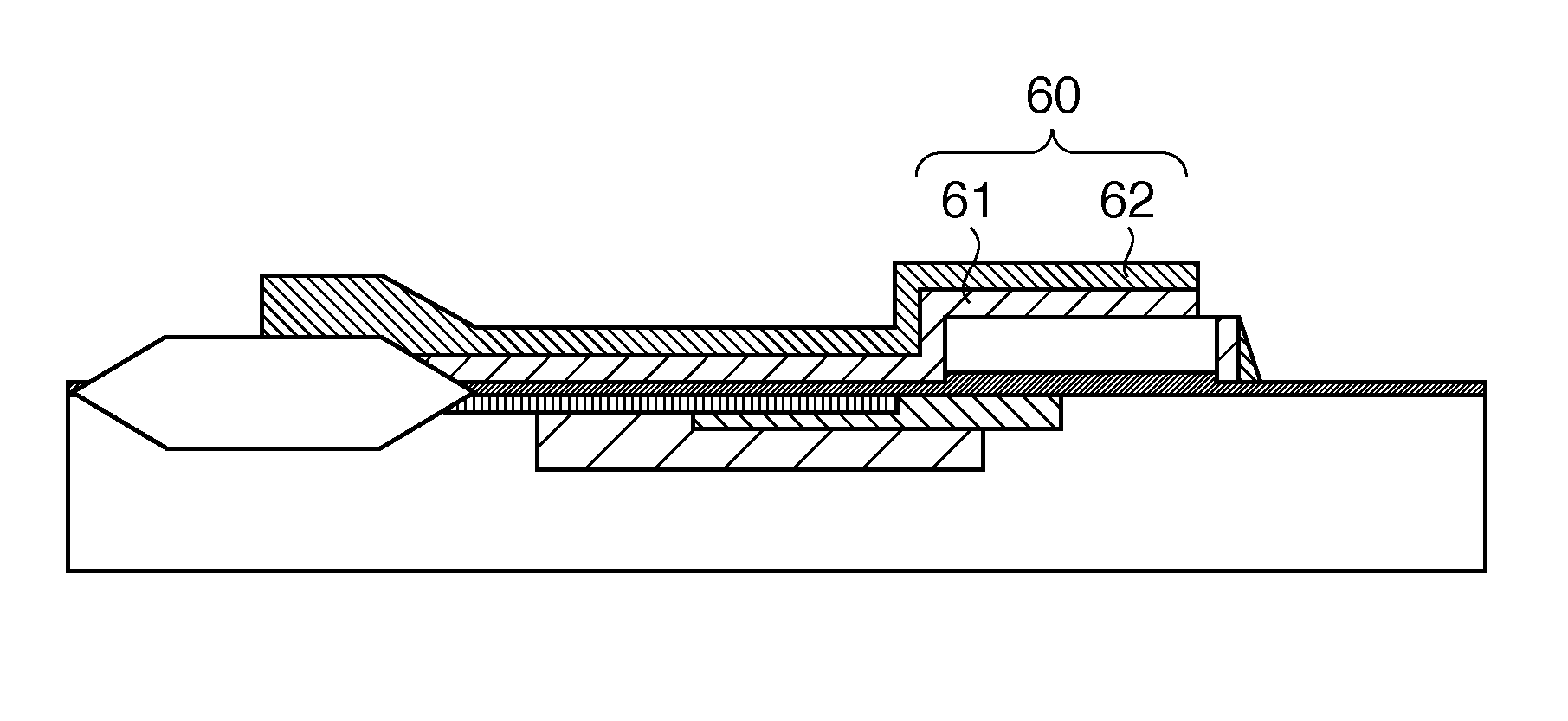
[0081]A different cross-sectional structure of a photodiode to which the manufacturing method of the present invention can be applied is illustrated in FIG. 3.

[0082]The following descriptions shall focus upon the differences with the first embodiment.

[0083]A photoelectric conversion apparatus 1j includes a pixel array PAj. Each pixel Pj within the pixel array PAj includes a photoelectric converting unit 51j. The photoelectric converting unit 51j further includes a transfer region 513j. The transfer region 513j is disposed laterally to the surface region 512. The transfer region 513j extends from between the charge storage region 511 and the surface region 512 toward the charge-voltage conversion unit 53. Accordingly, when the transfer transistor 52 is turned on, the charge stored in the charge storage region 511 can be easily transferred to the charge-voltage conversion unit 53. In other words, the efficiency of the charge transfer from the photoelectric converting unit 51j to the c...


PUM


Abstract

A manufacturing method for a solid-state image sensor, the method comprises the steps of: forming a charge storage region in a photoelectric converting unit by implanting a semiconductor substrate with ions of an impurity of a first conductivity type, using a first mask; heating the semiconductor substrate at a temperature of no less than 800° C. and no more than 1200° C. through RTA (Rapid Thermal Annealing); forming a surface region of the charge storage region by implanting the semiconductor substrate with ions of an impurity of a second conductivity type, using a second a mask; heating the semiconductor substrate at a temperature of no less than 800° C. and no more than 1200° C. through RTA (Rapid Thermal Annealing); and forming an antireflection film that covers the photoelectric converting unit at a temperature of less than 800° C., after the step of forming the surface region, in this order.

Description

BACKGROUND OF THE INVENTION[0001]1. Field of the Invention[0002]The present invention relates to a manufacturing method for a solid-state image sensor.[0003]2. Description of the Related Art[0004]Patent Document 1 (Japanese Patent Laid-Open No. 11-126893) discloses a photodiode, for configuring a solid-state image sensor, that includes a P-type charge storage layer and an N-type depletion prevention layer disposed thereupon. In order to form the stated P-type charge storage layer, a P-type semiconductor substrate is first implanted with boron ions, and is then heat-treated at a temperature of 800-1000° C. for approximately 30 minutes in a nitrogen atmosphere. Meanwhile, in order to form the stated N-type depletion prevention layer, a P-type semiconductor substrate is first implanted with phosphorous ions, and is then heat-treated at a temperature of 800-1000° C. for approximately 30 minutes in a nitrogen atmosphere. Patent Document 1 discloses that Rapid Thermal Annealing (RTA) may ...

Claims


Application Information

Patent Timeline
IPC IPC(8): H01L31/18H01L21/265
CPCH01L21/26513H01L21/324H01L27/14698H01L27/14643H01L27/14689H01L27/14621
Inventor HIROTA, KATSUNORIOHTANI, AKIRATASHIRO, KAZUAKIONUKI, YUSUKEWATANABE, TAKANORIICHIKAWA, TAKESHI
Owner CANON KK
Why Eureka
Try Eureka