
Solar cell

a solar cell and film technology, applied in the field of thin film solar cells, can solve the problems of glass substrates that cannot be easily damaged, so as to achieve low cost, low cost, and high peeling resistance.

Inactive Publication Date: 2010-10-07
FUJIFILM CORP
View PDF4 Cites 19 Cited by
  • Summary
  • Abstract
  • Description
  • Claims
  • Application Information

AI Technical Summary

Benefits of technology

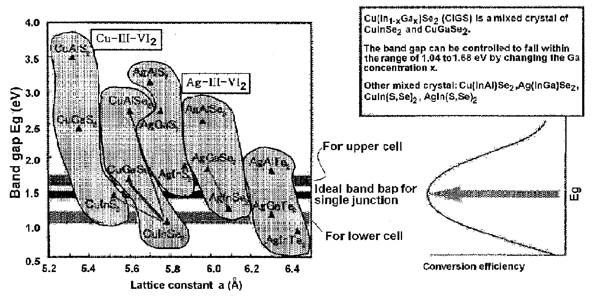
The present invention provides a solar cell that is lightweight, flexible, and has high thermal conductivity and peeling resistance. The cell has an optimized light absorption layer band gap and can increase efficiency with increased light utilization. The invention includes a metal substrate with an insulating anodic oxidation film and a photoelectric conversion layer. The anodic oxidation film has a surface roughness of 0.5 nm to 2 μm and the photoelectric conversion layer comprises a chalcopyrite semiconductor material with a band gap of 1.3 eV to 1.5 eV. The solar cell has pores with a pore size of 10 nm to 500 nm and the pores have a pore size of 10 nm to 200 nm. The anodic oxidation film has a textured surface structure defined by fractal analysis, wavelet analysis, or Fourier transform method. The photoelectric conversion layer can be made of semiconductor layers comprising elements such as copper, silver, indium, gallium, sulfur, selenium, and tellurium. The invention provides a solar cell that is efficient and durable.

Problems solved by technology

However, a glass substrate is fragile and must be treated with considerable care and its lack of flexibility limits the scope of the application.
However, a glass substrate would be even more fragile if it is thinned for reduction in weight.
If a metal is used as such a substrate material, its insulation from a solar cell material arranged thereon is difficult, while a resin substrate cannot withstand a high temperature exceeding 400° C. that is necessary to form a solar cell.
Furthermore, in a chalcopyrite material with higher light absorption efficiency, sufficient light cannot be confined, and incoming sunlight is not used effectively.

Method used

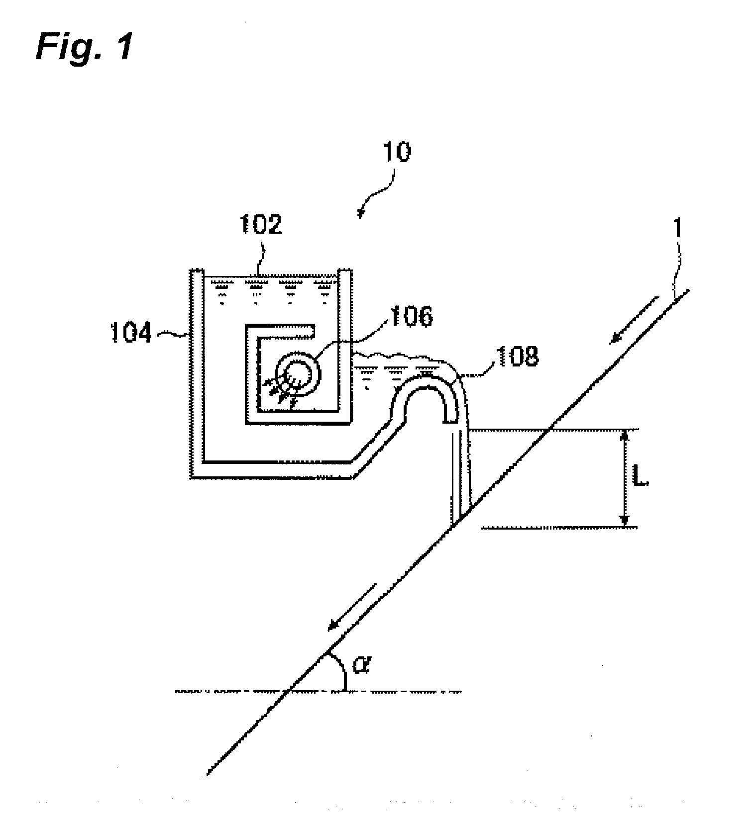

Image

  • Solar cell
  • Solar cell
  • Solar cell

Examples


example 1

[0389]The surface of the mechanically-polished, rolled aluminum sheet with a thickness of 0.24 mm was grained with a rotary nylon brush (6-10 nylon) and an aqueous suspension of 20% by weight of 400 mesh Pumice Stone (trade name, manufactured by Kyoritsu Ceramics Materials Co., Ltd.) and then thoroughly washed with water. The aluminum sheet was immersed in an aqueous 10% by weight sodium hydroxide solution (containing 5% by weight of aluminum) and so etched that aluminum was dissolved in an amount of 5 g / m2. Thereafter, the aluminum sheet was washed with running water, further neutralized with 20% by weight nitric acid, and then washed with water.

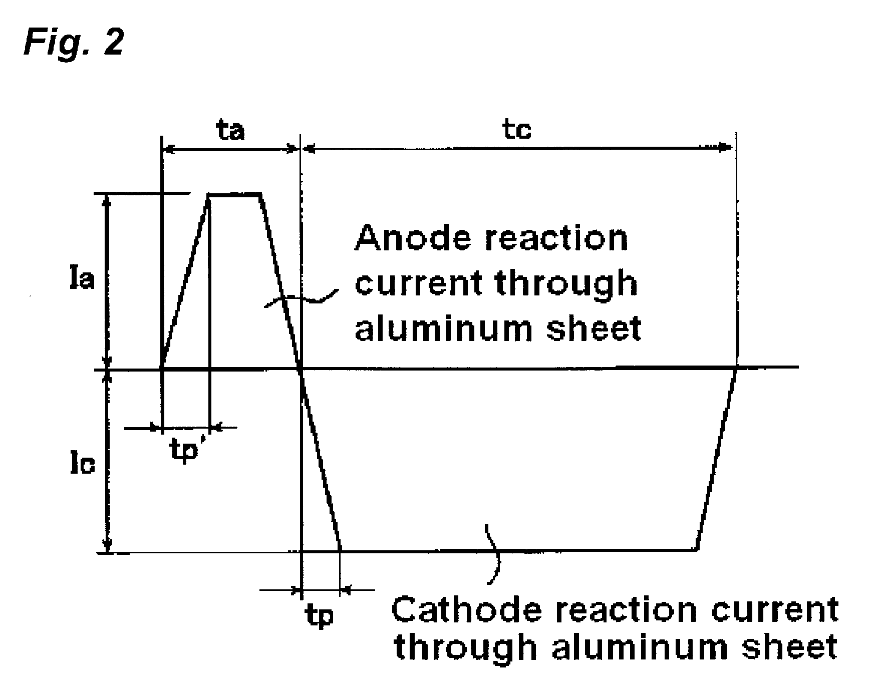
[0390]The aluminum sheet was then subjected to a surface roughening treatment with an anodic electric quantity of 160 Coulomb / dm2 in an aqueous 1% by weight nitric acid solution (containing 0.5% of aluminum) using a rectangular alternating waveform voltage with an anodic voltage of 10.5 V and a cathodic voltage of 9.3 V (current ratio r=0.9...

example 2

[0400]The sample of Example 1 according to the invention was used as a substrate. After a Mo layer was formed on the anodized aluminum substrate by RF sputtering (high frequency sputtering), a NaF layer was formed thereon by RF sputtering, and a Mo layer was further formed thereon by RF sputtering. The resulting Mo / NaF / Mo multilayer film had a thickness of about 1.0 μm. A CuInGaSe2 thin film was deposited on the Mo film in a vacuum chamber. In the deposition of the CuInGaSe2 thin film, a Cu (the primary component of CuInGaSe2) evaporation source, an In evaporation source, a Ga evaporation source, and a Se evaporation source were provided in the vacuum chamber 1, and the Cu, In, Ga, Se evaporation source crucibles were heated at the degree of vacuum of about 10−7 Torr so that each element was evaporated. In this process, the crucible temperature was controlled as needed. The CuInGaSe2 thin film was formed to have a two-layer structure as described below. The first layer of the two-la...

example 3

[0405]The surface of the mechanically-polished, rolled aluminum sheet with a thickness of 0.24 mm was grained with a rotary nylon brush (6-10 nylon) and an aqueous suspension of 20% by weight of 400 mesh Pumice Stone (trade name, manufactured by Kyoritsu Ceramics Materials Co., Ltd.) and then thoroughly washed with water. The aluminum sheet was immersed in an aqueous 10% by weight sodium hydroxide solution (containing 5% by weight of aluminum) and so etched that aluminum was dissolved in an amount of 5 g / m2. Thereafter, the aluminum sheet was washed with running water, further neutralized with 20% by weight nitric acid, and then washed with water.

[0406]The aluminum sheet was then subjected to a surface roughening treatment with an anodic electric quantity of 160 Coulomb / dm2 in an aqueous 1% by weight nitric acid solution (containing 0.5% of aluminum) using a rectangular alternating waveform voltage with an anodic voltage of 10.5 V and a cathodic voltage of 9.3 V (current ratio r=0.9...


PUM

PropertyMeasurementUnit
band gapaaaaaaaaaa
surface roughnessaaaaaaaaaa
roughnessaaaaaaaaaa

Abstract

A solar cell, comprising: a metal substrate having an insulating anodic oxidation film; and a photoelectric conversion layer provided on the metal substrate, whereon the anodic oxidation film has a surface roughness of 0.5 nm to 2 μm and the photoelectric conversion layer comprises a chalcopyrite semiconductor material having a band gap of 1.3 eV to 1.5 eV.

Description

TECHNICAL FIELD[0001]The present invention relates to thin-film solar batteries and more specifically to a lightweight, highly flexible thin-film solar cell produced with an anodized aluminum substrate.BACKGROUND ART[0002]Glass substrates are mainly used as thin-film solar cell substrates. However, a glass substrate is fragile and must be treated with considerable care and its lack of flexibility limits the scope of the application. Recently, solar batteries have attracted much attention as power supply sources to buildings including homes. It is inevitable to upsize solar batteries in order to ensure sufficient electric power to supply, and there has been a demand for a more lightweight substrate that should contribute to production of solar batteries with larger areas.[0003]However, a glass substrate would be even more fragile if it is thinned for reduction in weight. Therefore, there has been a demand for development of a less fragile and more flexible substrate material that can...

Claims


Application Information

Patent Timeline
Patent Type & Authority Applications(United States)
IPC IPC(8): H01L31/00
CPCH01L31/0749Y02E10/543Y02E10/541
Inventor YAGO, HARUOAONO, NARUHIKOHOSOYA, YOUICHISATO, TADANOBU
Owner FUJIFILM CORP
Learn More