Method for the production of semiconductor ribbons from a gaseous feedstock

Inactive Publication Date: 2010-12-16
SDSIL INVESTIGACAO E DESENVOLVIMENTO DE SOLUCOES SOLARES LDA
View PDF12 Cites 0 Cited by
  • Summary
  • Abstract
  • Description
  • Claims
  • Application Information

AI Technical Summary

Benefits of technology

[0035]The powder layer acts therefore simultaneously as (i) a substrate for the growth of the semiconduct

Problems solved by technology

Although easy to enunciate, and attractive in principle, this problem proved very difficult to solve: most silicon sheet growth techniques have failed to demonstrate sufficient conversion efficiency (particularly due to impurities and to crystallographic lattice imperfections), production reliability and low cost.
Although many methods have been proposed for the continuous, or semi continuous, growth of semiconductor ribbons, very few proved to be industrially viable.
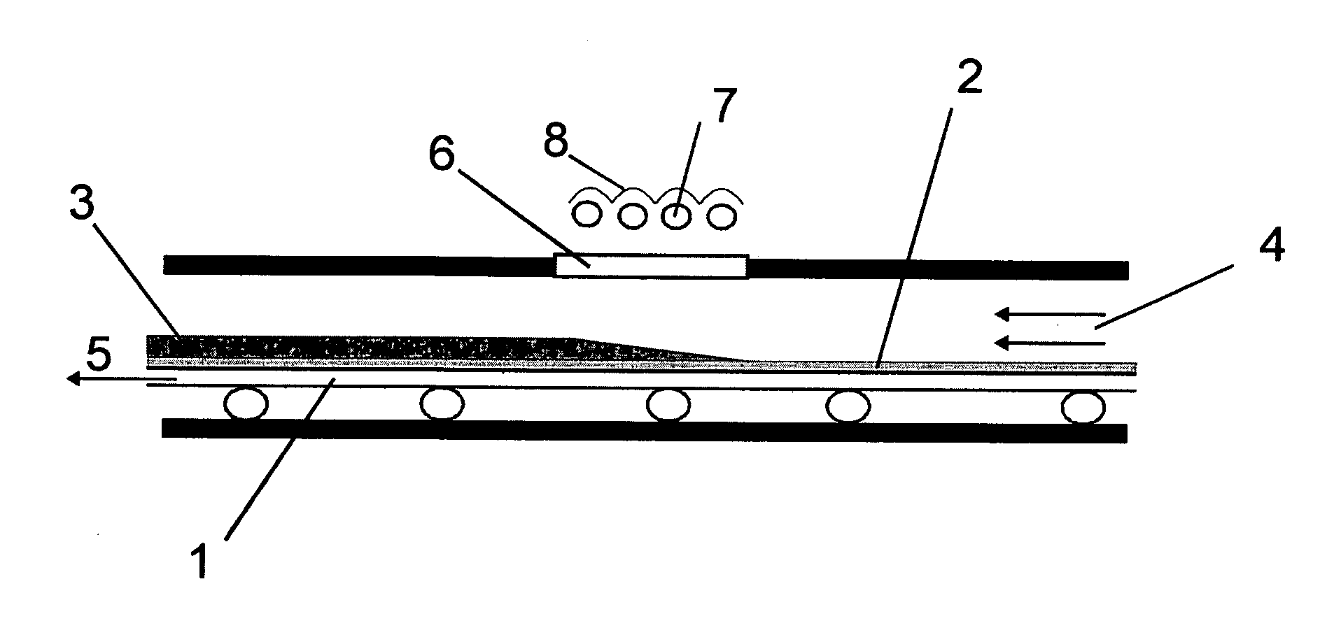
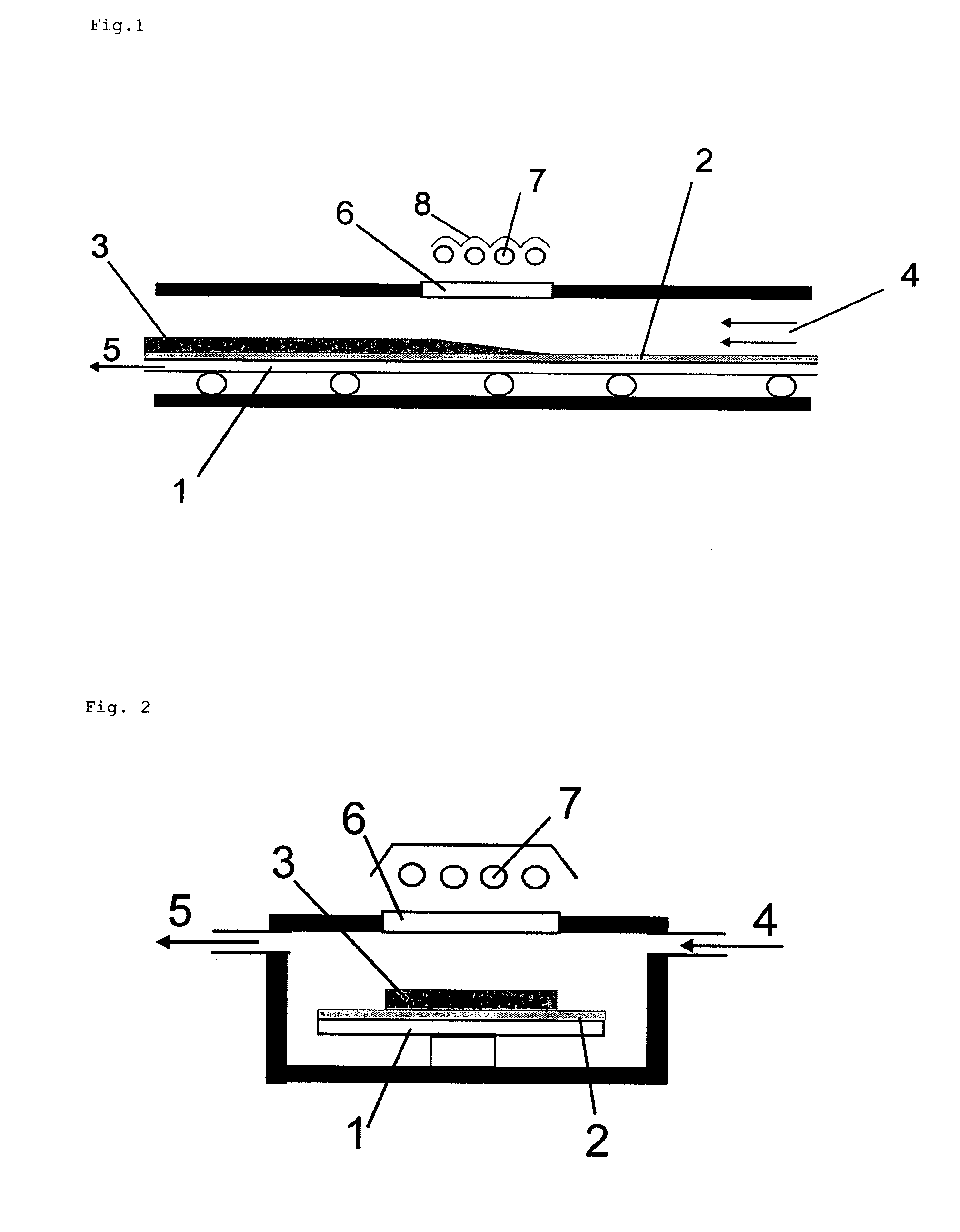
As we shall discuss below, the major difficulty in sheet production techniques that use a gaseous feedstock derive from the simple fact that a substrate is necessary: deposition of a solid plate from a gas requires a flat supporting surface.
Usually the deposited film will be strongly adhering to the substrate; since detachment is then impossible, a low cost substrate must be used, and resulting solar cells are usually low quality.
Detachment of grown films and re-use of high quality substrates is possible, by interposition of such sacrificial layers as electrochemical porous silicon, but costs are then high.
The main problems derive from the simple fact that silicon sheet formation from the gas phase needs a substrate.
Foreign substrates pose problems related to contamination, and to dislocation generation and plastic deformation due to thermally induced stress.
Despite numerous attempts, no foreign substrate process has proved outstandingly attractive so far.
Unfortunately, the results on cell quality versus process cost have not been sufficiently outstanding to encourage a fast path to an industrial phase.
On the contrary, high quality has been reached in films by epitaxial chemical vapour deposition at high temperatures on

Method used


Image

  • Method for the production of semiconductor ribbons from a gaseous feedstock
  • Method for the production of semiconductor ribbons from a gaseous feedstock

Examples


Example

[0042]The apparatus consists of a series of stages, corresponding to steps in the process. In the first stage, the gaseous feedstock, silane in hydrogen, is used to produce a fine powder of semiconductor material (silicon) by thermal decomposition in the gas phase. This semiconductor powder is uniformly spread and subsequently compressed and flattened, over a substrate constituted by contiguous quartz plates and moving at constant speed, by means of a vibrating blade and pressing piece.

[0043]In the next stage, represented in FIG. 1, the compressed and flattened powder layer (2) over the substrate (1) is heated by radiation from halogen lamps (7) through a quartz window (6). The gaseous feedstock (4) was made to flow over the heated surface, causing deposition of solid semiconductor material (3), silicon, over the heated surface. The deposited material thickens as the motion transports it under the radiation heaters.

[0044]In the third stage, the self-supporting (silicon) ribbon is de...


PUM

PropertyMeasurementUnit
Temperatureaaaaaaaaaa
Lengthaaaaaaaaaa
Fractionaaaaaaaaaa

Abstract

The present invention provides a method for the production of semiconductor ribbons using exclusively a gaseous feedstock. A fine powder of semiconductor material is produced by decomposition, within the gas phase, of a gaseous feedstock. A layer of this semiconductor powder is uniformly distributed, compressed and flattened over a planar substrate, which is continuously moving in one direction. This said layer of semiconductor powder is, in the following stage, heated to a temperature sufficient to decompose the said gaseous feedstock on its surface. A continuous flow of the said gaseous feedstock over said powder layer is ensured so that a solid plate of semiconductor material grows over the said layer of semiconductor powder. After the growth stage, during which the solid plate has grown to a convenient thickness, the said solid plate of semiconductor material is separated from the said layer of semiconductor powder and substrate. This self supporting plate is then heated to a high temperature in an atmosphere containing gaseous feedstock to complete its growth and become a ribbon with the appropriate structural properties for further processing. The present invention is applicable, for example, in the industry of silicon ribbon production for photovoltaic application.

Description

1. FIELD OF THE INVENTION[0001]The present invention relates to a process for the continuous growth of ribbons of semiconductor material from a gaseous feedstock.2. STATE OF THE ART[0002]Although the process here disclosed may apply to several semiconductor materials, presently the dominant material in the foreseen area of application (photovoltaics) is silicon, and we shall therefore refer especially to silicon in the following description of the state of the art.[0003]In all present industrial processes, silicon reaches the high purity grade (necessary to applications such as solar cells) as a gas of the silane family, SiH4-nCln. In mainstream processes, the gas is then thermally decomposed into solid silicon in the form of granules or bars, which constitute commercial solid silicon feedstock. This feedstock is molten in a furnace, and allowed to crystallize into ingots, which are then sawn into wafers. Alternatively, molten silicon may be made to crystallize directly into silicon...

Claims


Application Information

Patent Timeline
IPC IPC(8): C23C16/24C23C16/01
CPCC23C16/01C23C16/24C30B23/00C30B23/025C30B25/00C30B25/18C30B29/06C30B33/02
Inventor VALLERA, ANTONIOSERRA, JOAOALVES, JORGE MAIABRITO, MIGUEL
Owner SDSIL INVESTIGACAO E DESENVOLVIMENTO DE SOLUCOES SOLARES LDA
Why Eureka
Try Eureka