AI technical title is built by Patsnap AI team. It summarizes the technical point description of the patent document.
a technology of dielectric composition and resistance, which is applied in the manufacture of electrode systems, fixed capacitors, electric discharge tubes/lamps, etc., can solve the problems of uncontrollable charging induced emission and severely limit the anode voltage, and achieve the effect of reducing resistances
Inactive Publication Date: 2011-01-13
EI DU PONT DE NEMOURS & CO
View PDF29 Cites 1 Cited by
Summary
Abstract
Description
Claims
Application Information
AI Technical Summary
This helps you quickly interpret patents by identifying the three key elements:
Problems solved by technology
Method used
Benefits of technology
Benefits of technology
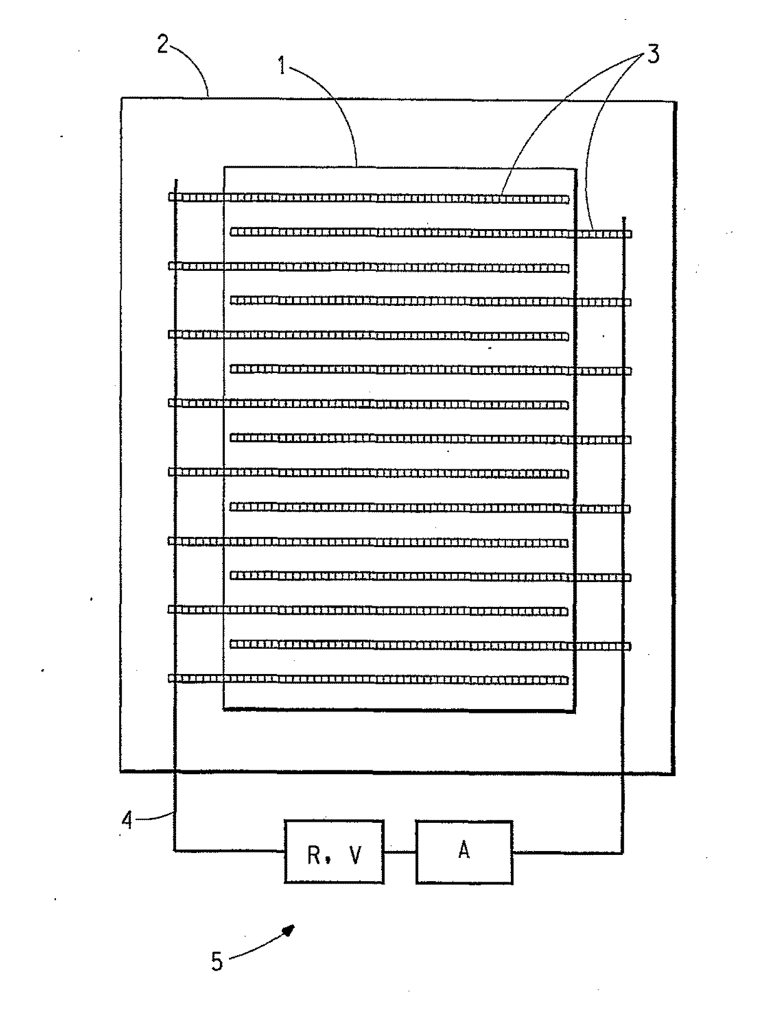
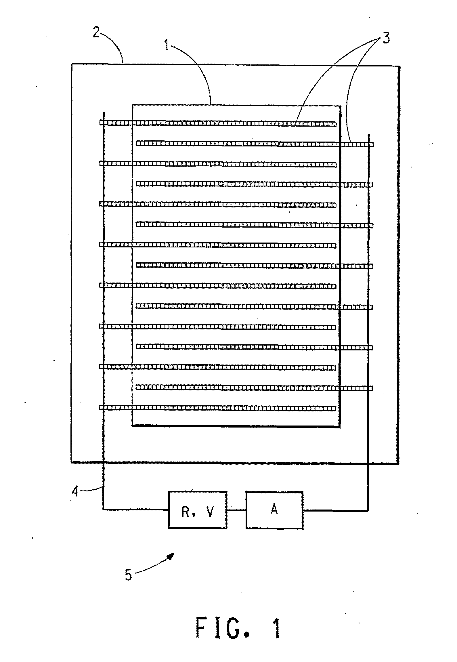
This patent describes a new dielectric composition that can be used in field emission devices. The composition includes a dielectric and a conductive oxide. The dielectric is fireable in air at a temperature between 450°C and 550°C. The conductive oxide can be selected from a variety of options, such as antimony-doped tin oxide or ruthenium dioxide. The amount of conductive oxide present should be between 0.25% and 25% of the total weight of the dielectric and conductive oxide. The dielectric composition should also be compatible with the treatment needed to form an electron emitter cathodeassembly. The patent also describes a paste for screen printing the dielectric composition. The dielectric composition has reduced resistances and is useful in field emission devices. The patent also provides a preferred dielectric and conductive oxide combination. The preferred conductive oxide is antimony-doped tin oxide.
Problems solved by technology
Since the static charge continues to build with time, uncontrollable charging induced emission can occur even at very low continuous anodevoltage.
Image
Click on the blue label to locate the original text in one second.
Reading with bidirectional positioning of images and text.
Examples
examples 1-4
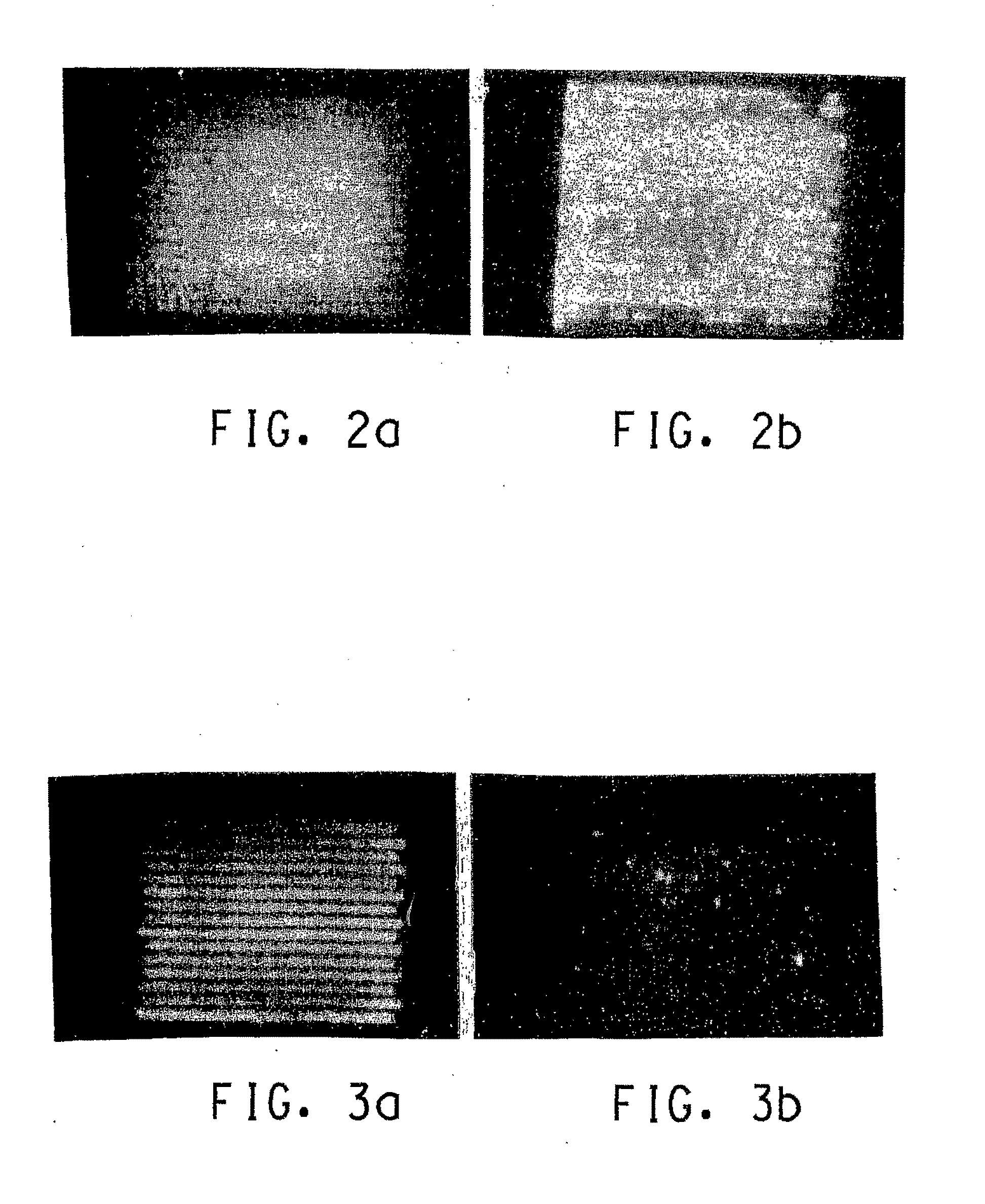
[0017]The purpose of these Examples was to compare various conductive oxides for the dielectric composition.
[0018]Four pastes were prepared using a bismuth-based dielectric frit and Cr2O3, V2O5, V2O3, and SnO2:Sb. The first three oxides were standard powder reagents. The antimony doped tin oxide, SnO2:Sb, was Zelec® ECP 3010-XC, which can be obtained from E. I. du Pont de Nemours and Company, Wilmington, Del.
[0019]The bismuth-based frit used in these Examples, Bi-frit, has the composition shown in Table I:
[0021]The vehicle is a standard thick film paste ingredient consisting of a mixture of 10% ethylcell...
examples 5-11
Comparative Experiments A-C
[0024]These Examples and Comparative Experiments show the effects of various amounts of the conductive oxide SnO2:Sb in eliminating the charging of the dielectric and the resulting undesirable electron emission.
[0025]The paste of Example 1 was blended with a paste with the composition shown in Table IV:
where the Bi-frit, vehicle, surfactant and pigment are identical to those used for the paste of Example 1. Ten different pastes were formed with SnO2:Sb content ranging from 0 to 10 wt % based on the total weight of the paste. The SnO2:Sb content of each Example and Comparative Experiment is shown in Table V below:
PUM
Property
Measurement
Unit
temperature
aaaaa
aaaaa
thick
aaaaa
aaaaa
resistance
aaaaa
aaaaa
Abstract
This invention provides a dielectric composition comprising a dielectric which is fireable in air at a temperature in the range of about 450° C. to about 550° C. and a conductive oxide selected from the group consisting of antimony-doped tinoxide, tin-doped indiumoxide, a transition metaloxide which has mixed valence states or will form mixed valence states after firing in a nitrogenatmosphere at a temperature in the range of about 450° C. to about 550° C. and normally conducting precious metal oxides such as ruthenium dioxide, wherein the amount of conductive oxide present is from about 0.25 wt % to about 25 wt % of the total weight of dielectric and conductive oxide. This dielectric composition has reduced electrical resistance and is useful in electron field emission devices to eliminate charging of the dielectric in the vicinity of the electron emitter and the effect of static charge induced field emission.
Description
FIELD OF THE INVENTION[0001]This invention provides a dielectric composition with reduced electrical resistance that is useful in electron field emission devices to eliminate charging of the dielectric in the vicinity of the electron emitter and the effect of static charge induced field emission.BACKGROUND OF THE INVENTION[0002]In certain designs of cathode plates for field emission devices, e.g., field emission displays, the layout of the cathode surface may require the emitter lines to be bordered by or in close proximity to electrically insolating dielectric surfaces. During field emission, these neighboring dielectric surfaces are bombarded by high energy electrons with shallow angle of incidence. As a result, secondary electron emission may occur from the dielectric surface leaving behind static positive charges. These positively charged surfaces, being only a short distance away from the emitter, will exert a large positive electric field on the emitter resulting in even stron...
Claims
Application Information
Patent Timeline
Application Date:The date an application was filed.
Publication Date:The date a patent or application was officially published.
First Publication Date:The earliest publication date of a patent with the same application number.
Issue Date:Publication date of the patent grant document.
PCT Entry Date:The Entry date of PCT National Phase.
Estimated Expiry Date:The statutory expiry date of a patent right according to the Patent Law, and it is the longest term of protection that the patent right can achieve without the termination of the patent right due to other reasons(Term extension factor has been taken into account ).
Invalid Date:Actual expiry date is based on effective date or publication date of legal transaction data of invalid patent.
Patent Type & AuthorityApplications(United States)

