

Semiconductor device and semiconductor device manufacturing method
a semiconductor device and semiconductor technology, applied in the field of semiconductor devices, can solve the problems of degrading device performance, affecting and affecting the performance of the device, so as to achieve uniform and stable rectifying properties, reduce conduction losses, and avoid deterioration of the smoothness of the interface.
- Summary
- Abstract
- Description
- Claims
- Application Information
AI Technical Summary
Benefits of technology
Problems solved by technology
Method used
Image

Examples
embodiment 1
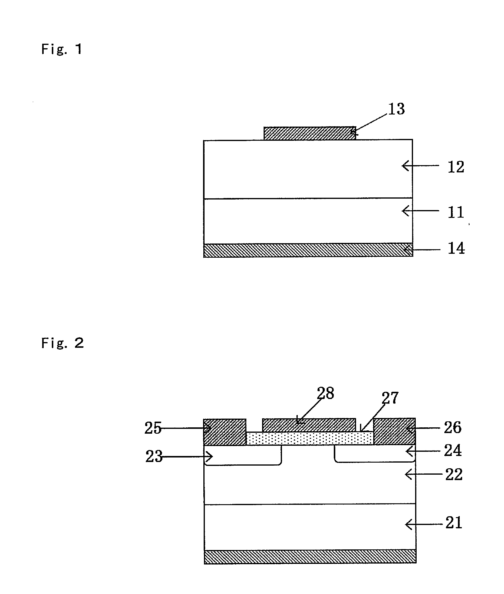
[0098]A Ni / 3C-SiC Schottky diode was fabricated according to the present invention. First, CVD was used to grow an n-type homoepitaxial layer with a carrier concentration of 3.0×10¹⁵ / cm3 on the (001) face of an n-type single-crystal cubic silicon carbide substrate with a carrier concentration of 3.0×10¹⁸ / cm3. The growth conditions were in accordance with Table 2. The thickness of the film grown was adjusted by controlling the growing time.
TABLE 2Conditions of homoepitaxial growth on single-crystal cubic siliconcarbide substrateGrowth temperature (° C.)1,600SiH4 flow rate (sccm)30C3H8 flow rate (sccm)17NH3 flow rate (sccm)1H2 flow rate (slm)2Pressure (Torr)10Thickness of film grown (micrometers)15
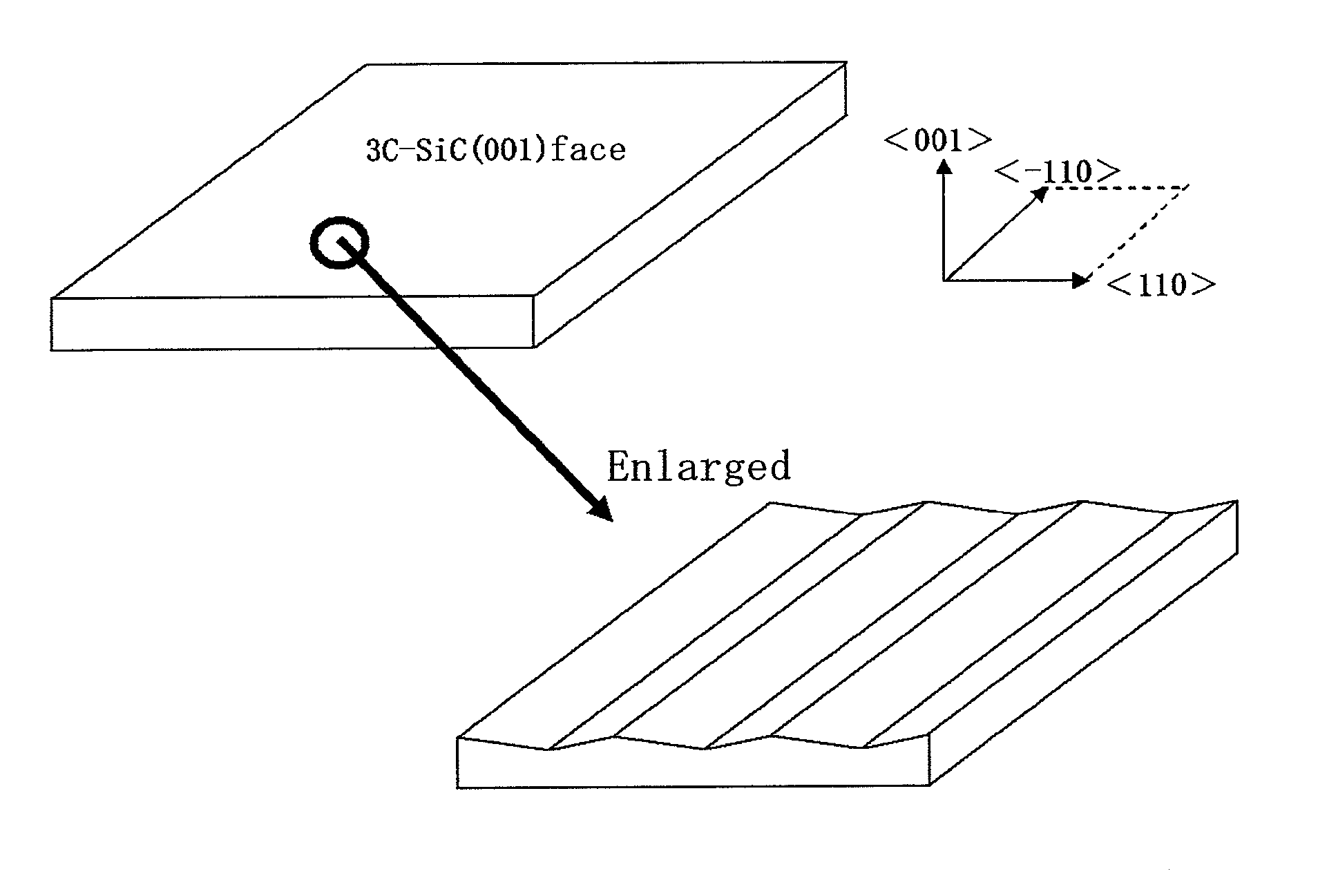
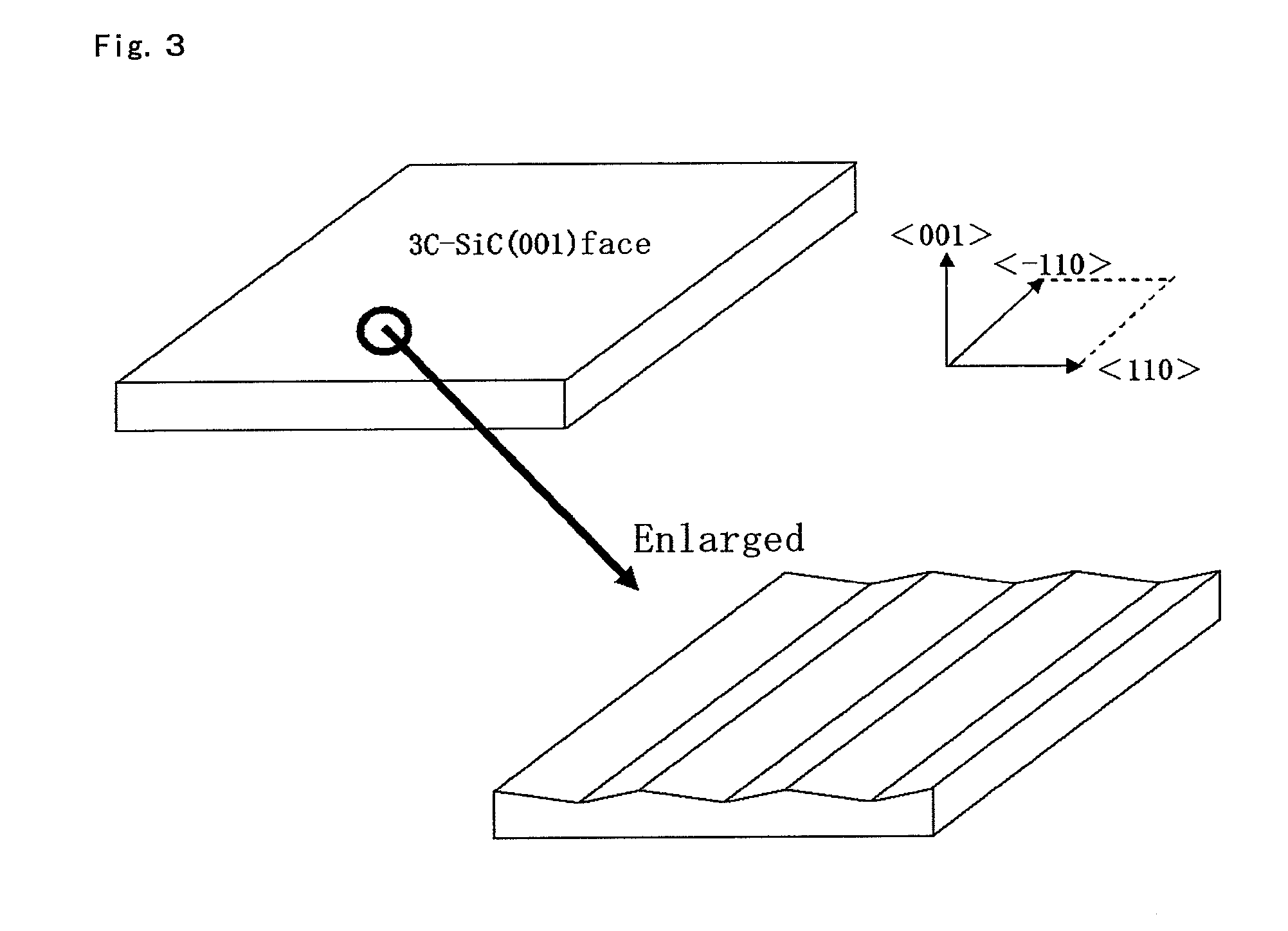
[0099]Next, diamond slurry with 1 micrometer in diameter were used to form abundant polishing grooves approximately parallel to the [−110] direction on the surface of the homoepitaxially grown cubic silicon carbide thin film. This step formed protrusions with the (111) face and (−1-11) face ...
embodiment 2
[0104]A Ni / 3C-SiC Schottky diode was fabricated according to the present invention.
[0105]Diamond slurry 1 micrometer in diameter were used to form abundant polishing grooves that were approximately parallel to the [110] direction on the surface of a cubic silicon carbide thin film that had been homoepitaxially grown using the same substrate, method, and conditions as in Embodiment 1. With this step, the surface of the cubic silicon carbide thin film was covered with protrusions with the (−111) and (1-11) faces as missoriented directions. However, following the polishing stage, there were disordered surfaces in addition to the ideal faces. The peak-valley height of the protrusions was about 2 nm, and the average distance between protrusion peaks was 1 micrometer.
[0106]Next, thermal oxidation, etching, immersion in dilute hydrofluoric acid solution, and rinsing (cleaning) were sequentially conducted by the same methods and under the same conditions as in Embodiment 1 to completely rem...
reference example 1
[0109]A Ni / 3C-SiC Schottky diode was fabricated by the following process as a reference example of the present invention. Diamond slurry 1 micrometer in diameter were used to form abundant polishing grooves that were approximately parallel to the [100] direction on the surface of a cubic silicon carbide thin film that had been homoepitaxially grown using the same substrate, method, and conditions as in Embodiment 1. With this step, the surface of the cubic silicon carbide thin film was covered with protrusions with the (110) and (−1-10) faces as missoriented directions. However, following the polishing stage, there were disordered surfaces in addition to the ideal faces. The peak-valley height of the protrusions was about 2 nm, and the average distance between protrusion peaks was 1 micrometer.
[0110]Next, thermal oxidation, etching, immersion in dilute hydrofluoric acid solution, and rinsing (cleaning) were sequentially conducted by the same methods and under the same conditions as ...
PUM
 Abstract
Description
Claims
Application Information