Semiconductor device and manufacturing method thereof

a technology of semiconductor devices and manufacturing methods, applied in the direction of semiconductor devices, basic electric elements, electrical appliances, etc., can solve the problems of increasing the generation of devices, affecting the efficiency of the device, so as to achieve the effect of increasing the length of the gate electrode and achieving the effect of high current driving power

Inactive Publication Date: 2011-02-10
RENESAS ELECTRONICS CORP
View PDF5 Cites 45 Cited by
  • Summary
  • Abstract
  • Description
  • Claims
  • Application Information

AI Technical Summary

Benefits of technology

[0008]The FINFET has a fin formed by processing a semiconductor layer. This fin is a region in a thin strip form (in the form of a rectangular solid) and both side-surface portions of the fin are used as channels of the FINFET. The gate electrode of the FINFET is formed over the both side surface portions of the fin so as to straddle over the fin. It has a so-called double gate structure. The FINEFT having such a configuration is superior to the MISFET having a conventional single gate structure from the standpoint of potential control of the channel region by the gate electrode. The FINFET has therefore advantages such as high punch-through resistance between a source region and a drain region and suppression of a short-channel effect even at a smaller gate length. Since the FINFET uses the both side surface portions of the fin as a channel, an area of the channel region through which a current is caused to flow can be made greater and a higher current driving power can be attained. This means that the FINFET is expected to satisfy both the suppression of a short-channel effect and securement of a high current driving power.
[0009]The FINFET has however difficulty in controlling its threshold voltage. For example, in the conventional planar type MISFET, its threshold voltage is controlled by adjusting the impurity concentration in the channel region. In this case, as the planar type MISFET becomes smaller, the concentration of an impurity to be introduced into the channel region becomes higher in accordance with the scaling law. This means that in the conventional planar type MISFET, size reduction decreases the distance between the source region and the drain region, tending to cause punch-through. The punch-through is therefore controlled by raising the impurity concentration of the channel formed between the source and the drain. An increase in the impurity concentration of the channel however increases the variation in the impurity concentration among elements, resulting in an increase in the variation in the characteristics of the planar type MISFET. In addition, it enhances impurity scattering due to carriers passing through the channel, causing deterioration in the mobility of the carriers.

Problems solved by technology

This dimensional reduction in the MISFET has been performed in accordance with the scaling law, but various problems have appeared as the generation of a device becomes greater.
It therefore becomes difficult to satisfy both the suppression of a short channel effect of a MISFET and securement of a high current driving power.
The FINFET has however difficulty in controlling its threshold voltage.
This means that in the conventional planar type MISFET, size reduction decreases the distance between the source region and the drain region, tending to cause punch-through.
In addition, it enhances impurity scattering due to carriers passing through the channel, causing deterioration in the mobility of the carriers.

Method used


Image

  • Semiconductor device and manufacturing method thereof
  • Semiconductor device and manufacturing method thereof
  • Semiconductor device and manufacturing method thereof

Examples


embodiment 1

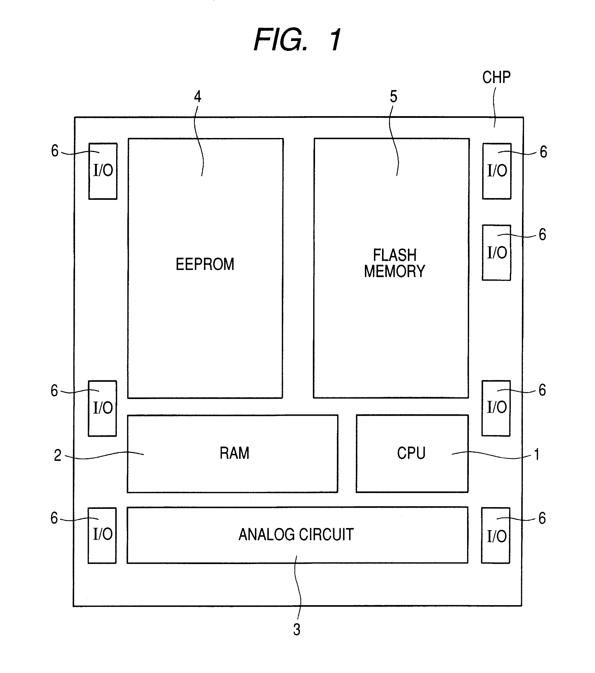
[0063]A semiconductor device according to Embodiment 1 will next be described referring to some drawings. First, the layout structure of a semiconductor chip having a system including a microcomputer will be described. FIG. 1 is a diagram illustrating the layout structure of a semiconductor chip CHP according to Embodiment 1. In FIG. 1, the semiconductor chip CHP has a CPU (central processing unit) 1, a RAM (random access memory) 2, an analog circuit 3, an EEPROM (electrically erasable programmable read only memory) 4, a flash memory 5, and an I / O (input / output) circuit 6.

[0064]The CPU (circuit) 1 is also called a central processing unit and is the heart of a computer or the like. The CPU1 fetches and decodes instructions from a memory device and based on them, it controls various operations or carries out a variety of arithmetic operations.

[0065]The RAM (circuit) 2 is a read / write memory. Stored information can be read randomly or written newly. It is also called a random access me...

embodiment 2

[0163]In Embodiment 1, as illustrated in FIG. 28, an n-type impurity such as phosphorus (P) or arsenic (As) is introduced into the source region SR1 and the drain region DR1 (including a portion of the fin FIN1 not covered with the gate electrode G1) formed in the n-channel FINFET formation region by using photolithography and oblique ion implantation. In short, ion implantation is employed as a method for introducing an impurity into the fin FIN1 not covered with the gate electrode G1. In this case, it is desired to lower the resistance of the fin FIN1 from the standpoint of improving the characteristics of the FINFET. It is necessary to control the dosage of an impurity and an implantation energy in order to lower the resistance of the fin FIN1.

[0164]FIG. 34 is a graph showing the relationship between the sheet resistance of the fin FIN1 and the dosage of an impurity introduced into the fin FIN1. In FIG. 34, the dosage of an impurity is plotted along the abscissa and the sheet res...


PUM


Abstract

To provide, in FINFET whose threshold voltage is determined essentially by the work function of a gate electrode, a technology capable of adjusting the threshold voltage of FINFET without changing the material of the gate electrode. FINFET is formed over an SOI substrate comprised of a substrate layer, a buried insulating layer formed over the substrate layer, and a silicon layer formed over the buried insulating layer. The substrate layer has therein a first semiconductor region contiguous to the buried insulating layer. The silicon layer of the SOI substrate is processed into a fin. A ratio of the height of the fin to the width of the fin is adjusted to fall within a range of from 1 or greater but not greater than 2. In addition, a voltage can be applied to the first semiconductor region.

Description

CROSS-REFERENCE TO RELATED APPLICATIONS[0001]The disclosure of Japanese Patent Application No. 2009-184285 filed on Aug. 7, 2009 including the specification, drawings and abstract is incorporated herein by reference in its entirety.BACKGROUND OF THE INVENTION[0002]The present invention relates to a semiconductor device and a manufacturing technology thereof, in particular, to a semiconductor device having a FINFET (FIN field effect transistor) and a technology effective when applied to a manufacturing technology thereof.[0003]Japanese Unexamined Patent Publication No. 2009-105122 (Patent Document 1) describes a technology for the purpose of providing a semiconductor device equipped with a FINFET excellent in characteristics by improving the processing accuracy of a fin or gate electrode forming the FINFET or improving the variation among a plurality of FINFETs. More specifically, it describes a semiconductor device obtained by forming a FINFET over an SOI (silicon on insulator) subs...

Claims


Application Information

Patent Timeline
Patent Type & Authority Applications(United States)
IPC IPC(8): H01L27/12H01L21/84
CPCH01L27/1211H01L21/845
Inventor IWAMATSU, TOSHIAKIISHIKAWA, KOZOHAYASHI, KIYOSHI
Owner RENESAS ELECTRONICS CORP
Why Eureka
Try Eureka