
Methods and apparatus for recovery of silicon and silicon carbide from spent wafer-sawing slurry

a technology of wafer cutting and recovery method, which is applied in the direction of separation process, furnace, other chemical processes, etc., can solve the problems of reducing the content of steel, reducing the efficiency of the value chain, and losing around 40-50% of the silicon during the wafer cutting process, so as to reduce the content of steel.

Inactive Publication Date: 2011-03-10
QUIXOTIC SYST
View PDF53 Cites 19 Cited by
  • Summary
  • Abstract
  • Description
  • Claims
  • Application Information

AI Technical Summary

Benefits of technology

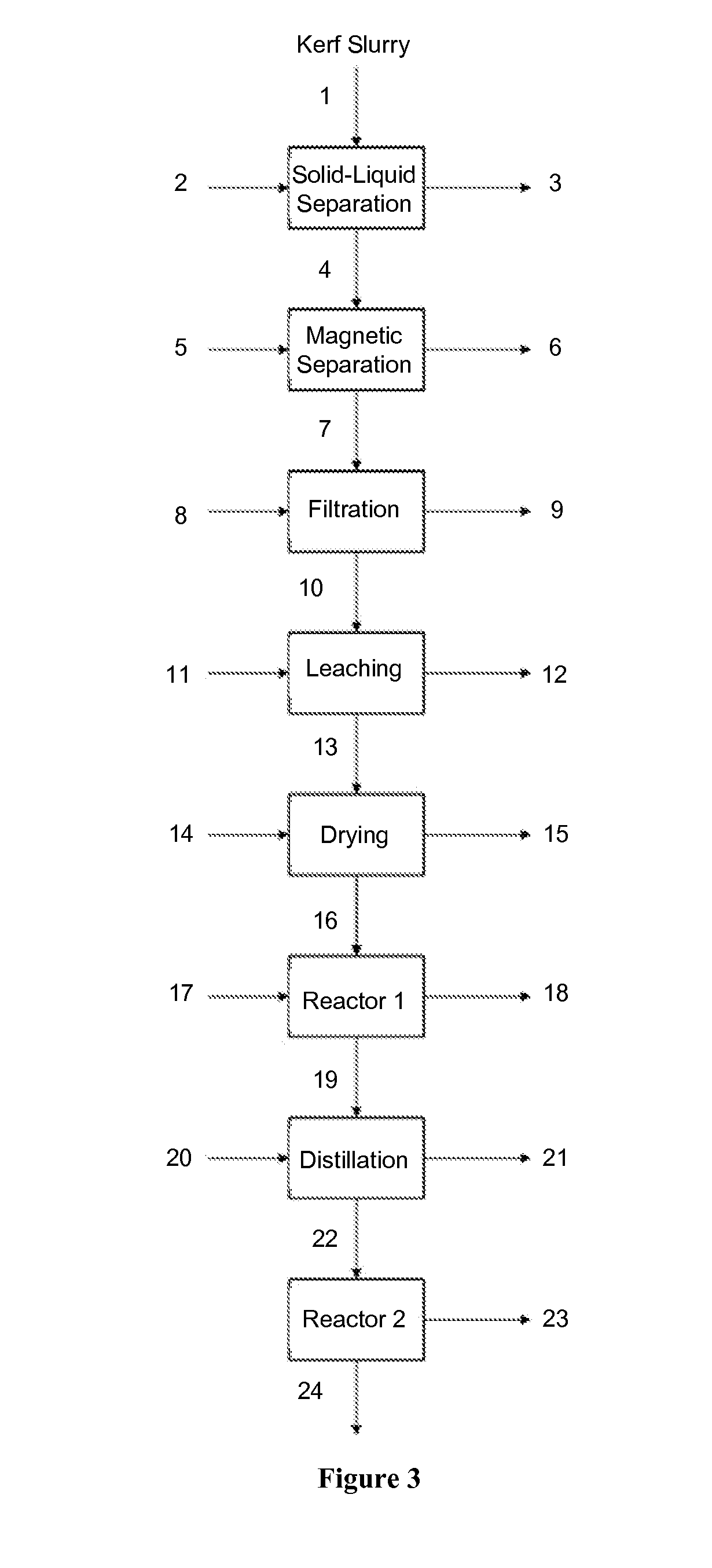
[0015]Other embodiments of the invention provide purification systems and methods, which can be used to produce high purity silicon, that can perform one or more of the following: (1) separation of large silicon carbide particles (e.g., particles greater than 5 micrometers in effective diameter) by means of gravity separation methods with or without the aid of centrifugal forces of different magnitude (e.g., settling tank, clarifier, hydro-cyclone, centrifuge, filter, and hydraulic classifier that uses additional convective flow to effect separation); (2) removal of wire-saw steel particles from the slurry using one or more series of magnetic separation devices (e.g., magnets or electromagnets); (3) performing leaching, e.g., by reacting the steel-depleted slurry with an acidic solution so as to further reduce the content of steel; (4) removal of a liquid phase (e.g., PEG) to produce a moist fine powder mixture (e.g., less than 5 percent liquid) of enriched-silicon with only minor amounts of steel and smaller-sized (e.g., less than 5 micrometers in effective diameter) silicon carbide parti...

Problems solved by technology

A serious shortcoming in the silicon-based PV value chain, however, is that there is a loss of around 40-50% of the silicon during the wafer cutting process.
However, this value chain is not without inefficiencies.
Therefore, while a raw material silicon shortage exists today for the PV industry that is driving prices toward the electronic-grade silicon (EG-Si) level, about half of all silicon produced for the ME and PV industries is being landfilled.
Although the silicon particles lost during this step are of the same purity as the original ingot, there exist no commercially viable technologies to recover and reuse this silicon.
Efforts to physically separate these silicon particles from the mixture are severely hampered by wire-saw particle impurities (mostly iron, copper, and zinc) that prevent the attainment of the original ingot purity.
Even if it were possible to completely remove the wire-saw particles from the slurry by physical means, the remaining ultrafine silicon powder is both dangerous to handle (due to potential dust explosions) and extremely difficult to melt using conventional furnace technology.
It has been well-documented that the solar industry has suffered from a major silicon feedstock shortage since 2005.1 During these past 4 years, more than 40% of the >100,000 tonnes of silicon produced during this timeframe was discarded due to the inability to recycle polysilicon.
This inefficient use of a critical PV cell building block resulted in a cumulative economic loss to the solar industry of at least $2 Billion over the period 2005-2008.2 Moreover, given that the cost of silicon feedstock comprises almost 20% of a PV cell's total cost3, discarding approximately 40% of the feedstock has been an important contributor to the economics preventing grid-parity and broader adoption of PV cells.

Method used


Image

  • Methods and apparatus for recovery of silicon and silicon carbide from spent wafer-sawing slurry
  • Methods and apparatus for recovery of silicon and silicon carbide from spent wafer-sawing slurry

Examples


example 1

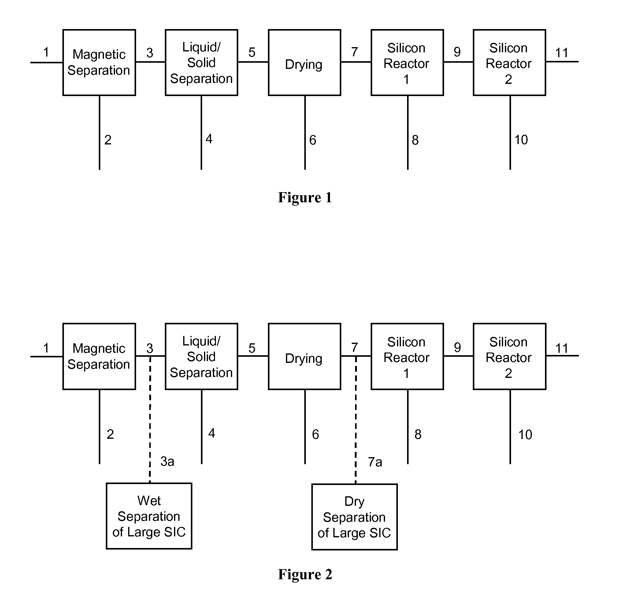
[0050]Two replicate experiments were performed in a bench-scale process system. The conditions used with apparatus (Reactor 1 and Reactor 2) in FIGS. 1 and 2 for Runs S1-31-08-11-14 and S1-31-08-12-05 are listed in Table 1 below.

TABLE 1Run S1-31-08-11-14Run S1-31-08-12-05Raw materials used inHigh purity iodine andHigh purity iodine andSiI4 productionsilicon wafer piecessilicon wafer piecesSi Source materialTreated industrial kerfTreated industrial kerf(Reactor 1)beadsbeadsDeposition zone bedQuartz slidesQuartz slidesmaterial (Reactor 2)Reactor 1 (° C.)12001200Reactor 2 (° C.) 900 900Carrier gasArgonArgon

[0051]Kerf raw material from an industrial source was subjected to a series of steps including magnetic separation, leaching, solid / liquid separation, and drying. Table 2 shows a comparison of the composition difference between Stream 1 and 7 in FIG. 1 using GDMS analysis. The Boron and Phosphorous composition of silicon product is given in Table 3. Finally, a representative sample o...


PUM

PropertyMeasurementUnit
Temperatureaaaaaaaaaa

Abstract

Methods, systems, and apparatus are disclosed herein for recovery of high-purity silicon, silicon carbide and PEG from a slurry produced during a wafer cutting process. A silicon-containing material can be processed for production of a silicon-rich composition. Silicon carbide and PEG recovered from the silicon-containing material can be used to form a wafer-saw cutting fluid. The silicon-rich composition can be reacted with iodine containing compounds that can be purified and / or used to form deposited silicon of high purity. The produced silicon can be used in the photovoltaic industry or semiconductor industry.

Description

CROSS-REFERENCE[0001]This application claims benefit of U.S. Provisional Application No. 61 / 044,342, filed Apr. 11, 2008, and U.S. Provisional Application No. 61 / 148,033, filed Jan. 28, 2009, which are each incorporated herein by reference in their entirety.FIELD OF INVENTION[0002]The invention relates to methods and systems for recovering silicon and silicon-containing compounds from spent slurry that is generated during wafer cutting or sawing operations in the microelectronic (ME) and photovoltaic (PV) industries. The invention relates to methods and systems that can produce a variety of useful products, including granular silicon products of high or increased purity. The products, such as granular silicon products of high or increased purity, can be suitable for multi-crystalline ingot casting or replacing electronic grade silicon (EG-Si) for single-crystal production in PV applications, and / or high-efficiency single-crystal solar cells. Other products can include fine silicon c...

Claims


Application Information

Patent Timeline
IPC IPC(8): C01B33/02B22F9/02C01B31/36C09K3/00B01J8/00B01J8/18
CPCC01B33/027B24B57/00B28D5/007Y02P70/10
Inventor FALLAVOLLITA, JOHN ALLAN
Owner QUIXOTIC SYST
Learn More