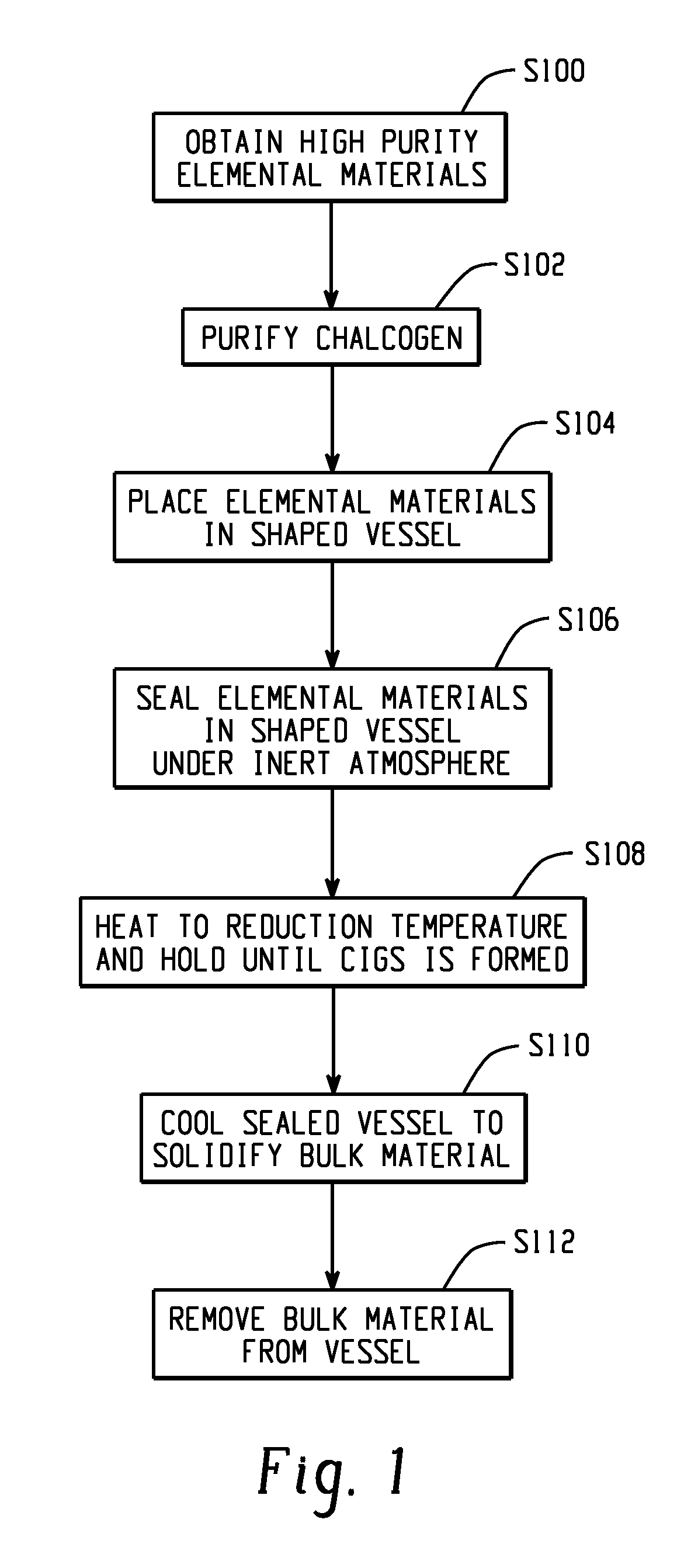
Synthesis of high-purity bulk copper indium gallium selenide materials
a technology of copper indium gallium selenide and high-purity bulk, which is applied in the direction of electrolysis components, vacuum evaporation coatings, coatings, etc., can solve the problems of limited solar power conversion efficiency into electricity of such devices, and no effective method for bulk production of cigs materials, etc., and achieve the effect of efficient devices
- Summary
- Abstract
- Description
- Claims
- Application Information
AI Technical Summary
Benefits of technology
Problems solved by technology
Method used
Image

Examples
example 1
Preparation of Bulk Cu1Ga1Se2 Material (x=0) at Low Temperature
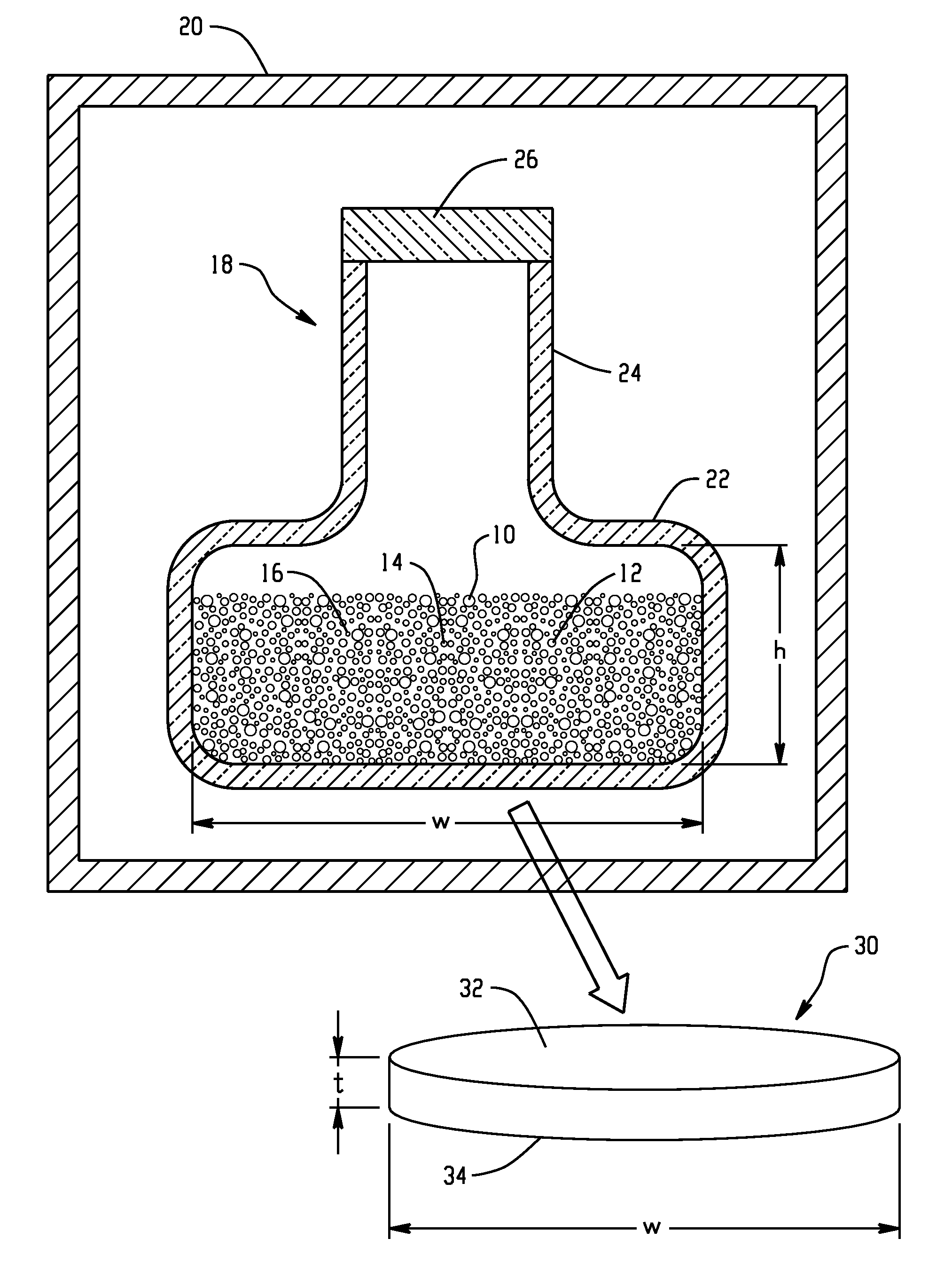
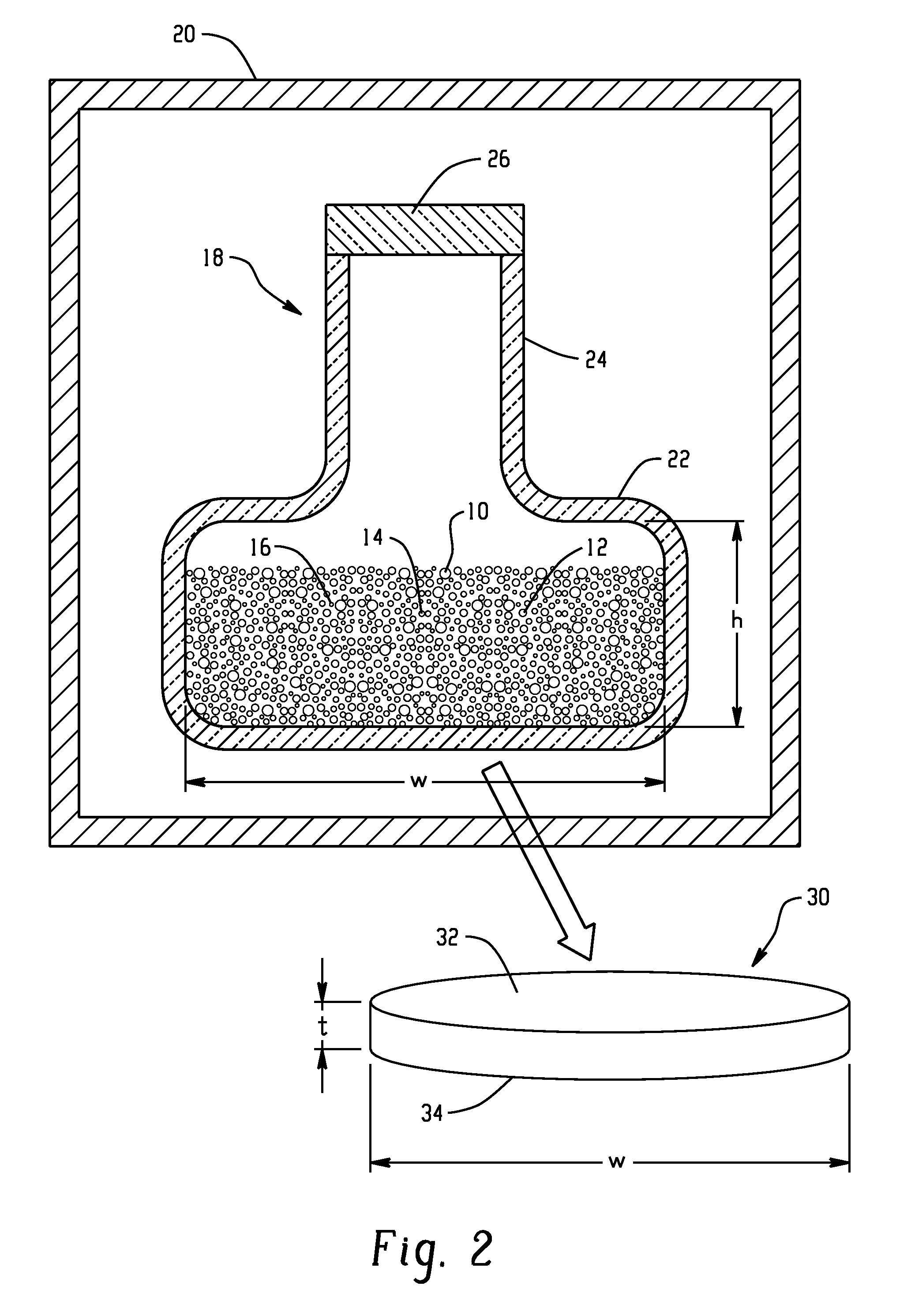
[0045]21.8229 grams of copper, 23.9442 grams of gallium, and 54.2328 grams of selenium (approximately 100.00 grams in total) were batched in a cylindrical silica ampoule inside a nitrogen atmosphere glove box. The ampoule was about 27 cm in total length and about 3 cm in internal width of a base portion, with an inlet portion of a narrower width and a length of about 4.5 cm. The ampoule was evacuated for 4 hours at a pressure of 1×10⁻⁵ Torr and then the inlet portion was sealed using a methane / oxygen torch.
[0046]The ampoule was placed in a furnace. The preparation schedule used for making 100 grams of bulk Cu1Ga1Se2 is given in Table I. At the end of the preparation schedule, the ampoule was removed from the furnace at room temperature and broken open inside a glove box under a nitrogen atmosphere to retrieve the bulk Cu1Ga1Se2 material.
TABLE IPreparation schedule for low temperature routeStepConditionsRamp 15°C. / minSoak...
example 2
Preparation of Bulk Cu In0.7Ga0.3Se Material x=0.3 at Low Temperature
[0048]25.596 grams of copper, 32.373 grams of indium, 8.425 grams of gallium, and 63.606 grams of selenium (approximately 130.00 grams in total) were batched in a silica ampoule as for Example 1. The ampoule was evacuated for 5 hours at a pressure of 1×10⁻⁵ Torr. The ampoule was sealed using a methane / oxygen torch and placed in a furnace, as for Example 1. The preparation schedule for preparing 130 grams of Cu1In0.7Ga0.3Se2 composition through the low temperature method was as shown in Table I. At the end of the preparation schedule, the ampoule was removed from the furnace at room temperature and broken open to retrieve the bulk Cu1In0.7Ga0.3Se2 material.
[0049]FIG. 6 shows an X-ray diffraction plot of the low-temperature prepared Cu1In0.7Ga0.3Se2 material above a reference profile. The X-ray pattern shows very high phase purity.
example 3
Procedure to Make Bulk Cu1In0.7Ga0.3Se2 Material (x=0.3) at High Temperature
[0050]5.906 grams of copper, 7.474 grams of indium, 1.944 grams of gallium, and 14.678 grams of selenium (approximately 30.00 grams in total) were batched in a silica ampoule. The ampoule was evacuated for 5 hours at a pressure of 1×10⁻⁵ Torr. The ampoule was then sealed using a methane / oxygen torch and placed in a furnace at a 45 degree angle. The preparation schedule used in making 100 grams of bulk Cu1Ga1Se2 composition was as given in Table 2. (The same process may be used for making 130 grams of Cu1In0.7Ga0.3Se2 composition, using material quantities as given in Example 2.) At the end of the preparation schedule, the ampoule was removed from the furnace at room temperature and broken open to retrieve the bulk Cu1In0.7Ga0.3Se2 material.
TABLE 2Preparation schedule for high temperature routeStepConditionsRamp 15°C. / minSoak Temperature A500°C.Soak Time at3hrs.Temperature ARamp 22°C. / minSoak Temperature B210...
PUM
| Property | Measurement | Unit |
|---|---|---|
| temperature | aaaaa | aaaaa |
| temperature | aaaaa | aaaaa |
| temperature | aaaaa | aaaaa |
Abstract
Description
Claims
Application Information
PatSnap Eureka turns technology decisions into work you can execute. Powered by our Innovation Knowledge Graph, it runs expert workflows across engineering, life sciences, materials and intellectual property. Get your review-ready output in minutes.


