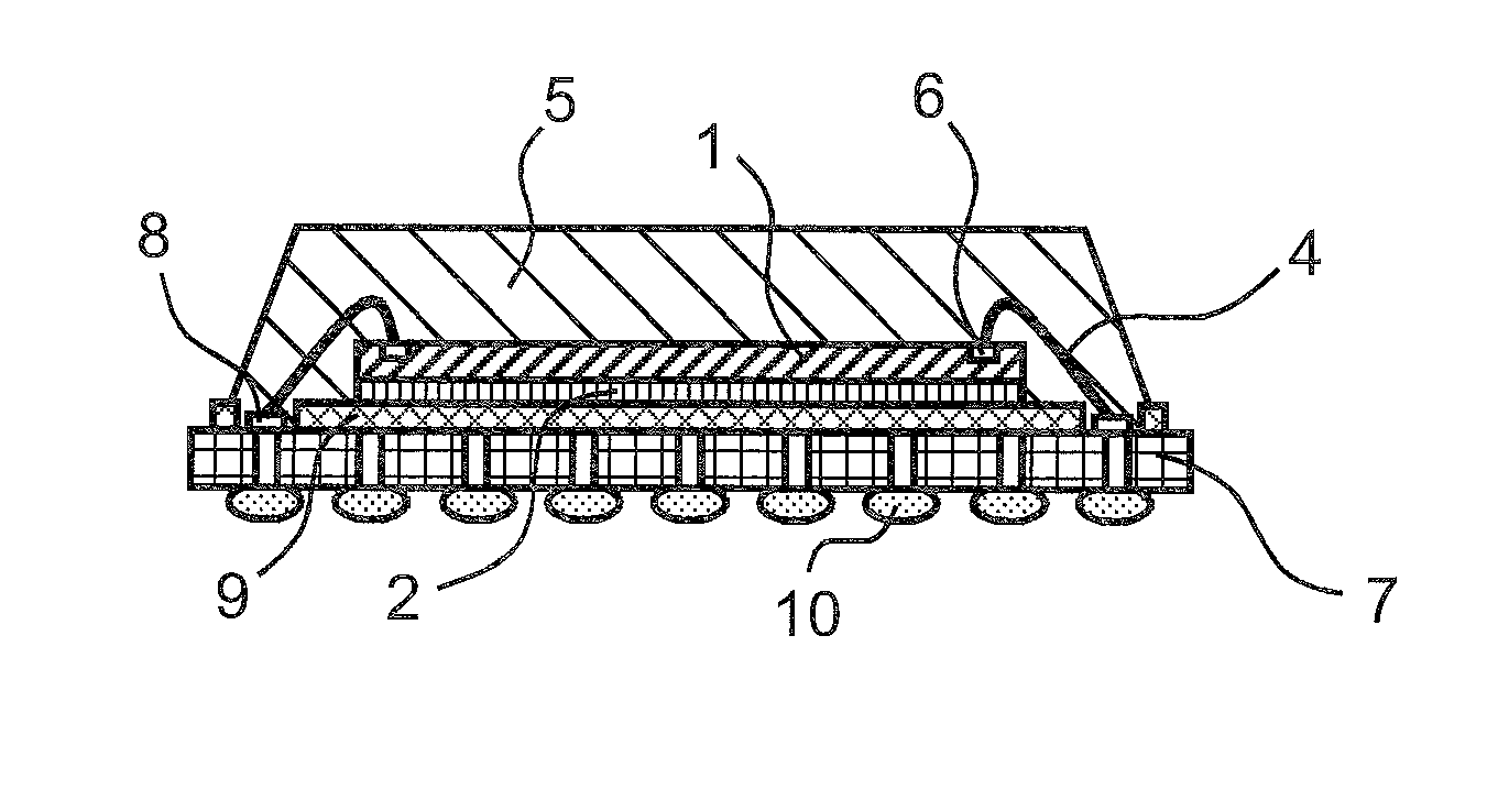
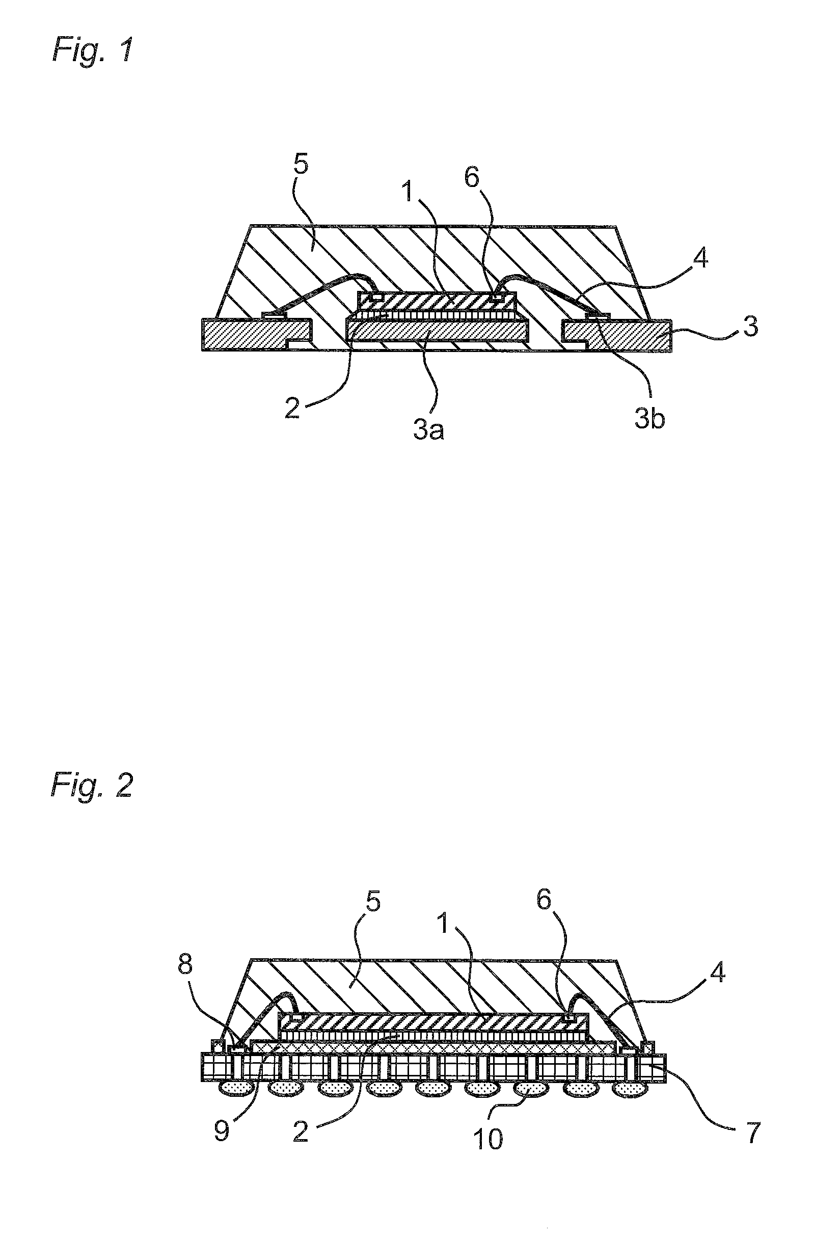
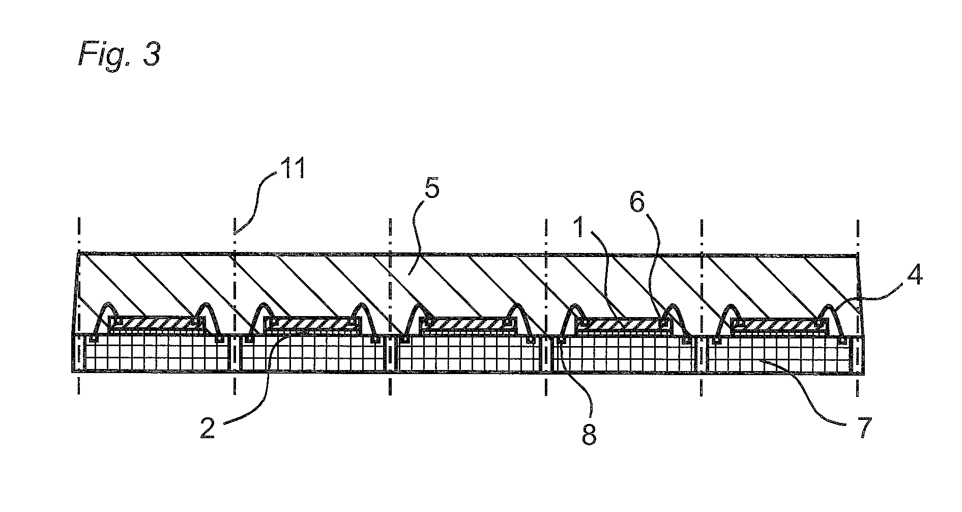
Semiconductor device

a technology of semiconductor devices and semiconductors, applied in semiconductor devices, semiconductor/solid-state device details, electrical devices, etc., can solve the problems of insufficient high-temperature storage life of semiconductor devices using such bonding wires made of metals other than gold, and high cost of conventional gold wire connection, so as to achieve excellent high-temperature storage life, migration resistance, and moisture resistance reliability. good balan

Inactive Publication Date: 2011-04-21
SUMITOMO BAKELITE CO LTD
View PDF10 Cites 39 Cited by
  • Summary
  • Abstract
  • Description
  • Claims
  • Application Information

AI Technical Summary

Benefits of technology

[0046]According to the present invention, there can be obtained the first semiconductor device in which the copper wire electrically connecting the electrical joints provided on the lead frame or the circuit board to the electrode pad provided on the semiconductor element is difficult to corrode, and whose solder resistance, high temperature storage life, high temperature operating life, migration resistance, and moisture resistance reliability are better balanced.
[0047]There can also be obtained the second semiconductor device which comprises the lead frame or the circuit board, the semiconductor element, and the encapsulating member, wherein the electrical joints provided on the lead frame or the circuit board and the electrode pad provided on the semiconductor element are connected by the copper wire, and which is excellent in high temperature storage life, high temperature operating life, and moisture resistance reliability.
[0048]Furthermore, there can be obtained the third semiconductor device which can exhibit excellent temperature cycle property, high temperature storage life, high temperature operating life, and moisture resistance reliability, even when the semiconductor element is provided with the electrode pad having a thickness of 1.2 μm or more.

Problems solved by technology

Furthermore, because the demand for cost reduction on semiconductor devices is also strict and the cost of the conventional gold wire connection is high, joining with use of metals such as aluminum, a copper alloy, and copper is employed in part.
However, the semiconductor devices using such bonding wires made of metals other than gold are still insufficient in the high temperature storage life and high temperature operating life under the high temperature environment having a temperature exceeding 150° C., which are especially demanded in the automotive applications, and electric reliability such as the moisture resistance reliability under the high temperature and high humidity environment having a temperature exceeding 60° C. and a relative humidity exceeding 60% RH.
Accordingly, there are problems such as migration, corrosion, and rise in electrical resistance, and thus satisfactory devices have not always been obtained.
Especially, in the semiconductor devices using copper wires, there is a problem that copper is easy to corrode in a moisture resistance reliability test and thus lacks in reliability.
Therefore, although copper wires have been successfully used as wires with a large wire diameter for discrete power devices and the like, it is currently difficult to employ copper wires for ICs requiring wires with a wire diameter of 25 μm or less, especially for single-sided encapsulated packages whose wires are even affected by impurities attributable to a circuit board.
Although there have been proposals focusing on only the copper wire as described above, corrosion and electric reliability such as moisture resistance reliability of a package encapsulated by a resin, i.e., a semiconductor device are not accounted for, and thus the proposals have not necessarily been satisfactory.
Such decrease in pitch of wires has had a problem that large capacitance is formed between the wires, which causes propagation delay of signals.
However, there has been a problem that the low dielectric insulating film generally has low mechanical strength, and in a conventional semiconductor device, cracking occurs in the low dielectric insulating film under the electrode pads provided on the semiconductor element due to impact during wire bonding, and thus they are less durable, especially under high temperature and high humidity.
However, in the conventional semiconductor devices using copper wires, since greater thickness of an electrode pad of a semiconductor element tends to lead to degradation of the high temperature storage life, high temperature operating life, and moisture resistance reliability, the semiconductor element has generally been provided with an electrode pad having a thickness of less than 1.2 μm.

Method used


Image

  • Semiconductor device
  • Semiconductor device
  • Semiconductor device

Examples


examples

[0190]Hereinafter, the present invention will be more concretely described based on the examples and comparative examples. However, the present invention is not limited to the following Examples.

[0191]First, the first semiconductor device of the present invention will be described based on Examples A1 to A30 and Comparative Examples A1 to A10. Components of the epoxy resin compositions used herein are described below.

[0192]

[0193]E-1: Biphenyl type epoxy resin (epoxy resin represented by the formula (3) in which R11's in the 3-position and 5-position are each a methyl group and R11's in the 2-position and 6-position are each a hydrogen atom, “YX-4000H” available from Japan Epoxy Resins Co., Ltd., melting point 105° C., epoxy equivalent 190, chlorine ion content 5.0 ppm)

[0194]E-2: Bisphenol A type epoxy resin (epoxy resin represented by the formula (4) in which R12 is a hydrogen atom and R13 is a methyl group, “YL-6810” available from Japan Epoxy Resins Co., Ltd., melting point 45° C....

example a1

[0224]The epoxy resin E-3 (8 parts by mass), the curing agent H-3 (6 parts by mass), the fused spherical silica 2 (85 parts by mass) as a filler, the compound 1 containing a sulfur atom (0.05 parts by mass), triphenylphosphine (0.3 parts by mass) as a curing accelerator, epoxysilane (0.2 parts by mass) as a coupling agent, carbon black (0.25 parts by mass) as a coloring agent, and carnauba wax (0.2 parts by mass) as a mold release agent were mixed at ordinary temperature using a mixer and then roll-milled at 70 to 100° C. After cooling, the resultant was pulverized to give an epoxy resin composition for an encapsulating member.

examples a2

to A30

[0225]Epoxy resin compositions for encapsulating members were prepared in the same manner as in Example A 1, except that the formulations were changed to those shown in Tables 1 to 6.


PUM


Abstract

A semiconductor device comprises a lead frame having a die pad portion or a circuit board, one or more semiconductor elements mounted on the die pad portion of the lead frame or on the circuit board, a copper wire that electrically connects electrical joints provided on the lead frame or the circuit board to an electrode pad provided on the semiconductor element, and an encapsulating member which encapsulates the semiconductor element and the copper wire, wherein the electrode pad and/or the encapsulating member having predetermined properties are combined with the copper wire having predetermined properties.

Description

TECHNICAL FIELD[0001]The present invention relates to a semiconductor device, and more particularly to a semiconductor device comprising a lead frame or a circuit board, a semiconductor element mounted on the lead frame or the circuit board, a copper wire that electrically connects electrical joints provided on the lead frame or the circuit board to an electrode pad provided on the semiconductor element, and an encapsulating member which encapsulates the semiconductor element and the copper wire.BACKGROUND ART[0002]Conventionally, electronic parts such as diodes, transistors, and integrated circuits are largely encapsulated by a cured product of an epoxy resin composition. Especially for the integrated circuits, epoxy resin compositions with excellent thermal and moisture resistance are used, the epoxy resin compositions containing epoxy resins, phenol resin-based curing agents, and inorganic fillers such as fused silica and crystalline silica. In recent years, however, in the marke...

Claims


Application Information

Patent Timeline
Patent Type & Authority Applications(United States)
IPC IPC(8): H01L23/28H01L23/495
CPCH01L21/565H01L23/3107H01L23/3128H01L23/4952H01L23/49548H01L24/43H01L24/45H01L24/97H01L2224/05664H01L2224/32225H01L2224/32245H01L2224/4312H01L2224/4321H01L2224/45015H01L2224/45147H01L2224/45565H01L2224/45664H01L2224/48091H01L2224/48227H01L2224/48247H01L2224/48465H01L2224/73265H01L2224/97H01L2924/01004H01L2924/01005H01L2924/01006H01L2924/01007H01L2924/01009H01L2924/01012H01L2924/01013H01L2924/01014H01L2924/01015H01L2924/01016H01L2924/01018H01L2924/0102H01L2924/01022H01L2924/01027H01L2924/01029H01L2924/0103H01L2924/01033H01L2924/01038H01L2924/0104H01L2924/01046H01L2924/01047H01L2924/0105H01L2924/01056H01L2924/01059H01L2924/01075H01L2924/01077H01L2924/01078H01L2924/01079H01L2924/01082H01L2924/01083H01L2924/01105H01L2924/01202H01L2924/01204H01L2924/01205H01L2924/14H01L2924/15311H01L2924/20752H01L2924/30105H01L24/48H01L2924/01019H01L2924/01023H01L2924/01043H01L2924/01045H01L2924/01055H01L2924/01067H01L2924/01072H01L2924/014H01L2224/45124H01L2224/45144H01L2924/12041H01L2224/48864H01L2224/48664H01L2224/48599H01L2224/48699H01L23/495H01L2924/1301H01L2924/01017H01L2224/82H01L2224/85H01L2924/00014H01L2924/00011H01L2224/83H01L2924/00H01L2924/00012H01L2924/00015H01L2924/013H01L2924/181H01L2224/48764H01L2224/05624H01L2224/05644H01L2224/05647H01L2924/12042H01L2224/48824H01L2224/48844H01L2224/48847H01L24/73H01L2924/0002H01L2924/20753H01L2924/20755H01L2924/20754H01L2924/2075H01L2924/01049H01L23/28H01L23/48
Inventor ZENBUTSU, SHIN-ICHIITOH, SHINGO
Owner SUMITOMO BAKELITE CO LTD
Why Eureka
Try Eureka