Sputtering target, transparent conductive film and transparent electrode

Active Publication Date: 2011-05-26
IDEMITSU KOSAN CO LTD
View PDF11 Cites 23 Cited by
  • Summary
  • Abstract
  • Description
  • Claims
  • Application Information

AI Technical Summary

Benefits of technology

[0101]As examples of the compound of indium, indium oxide, indium hydroxide or the like can be given.
[0102]As examples of the compound of tin, tin oxide, tin hydroxide or the like can be given.
[0103]As examples of the compound of zinc, zinc oxide, zinc hydroxide or the like can be given.
[0104]In view of readiness in sintering and suppression of generation of bi-products, oxides are preferable as the compound.
[0105]It is preferable to homogeneously blend and pulverize the metal ox

Problems solved by technology

Although ITO has excellent properties as a material for transparent conductive oxide, ITO is not only a scarce resource, but also contains a large amount (about 90 atomic percent) of indium which is a biologically harmful element.
If an abnormal electrical discharge occurs, scattered materials become attached to the transparent conductive oxide as impurities during or immediately after the film formation.
The indium content in ITO must be reduced due to these problems of instability of supply (scarcity), hazardous properties and occurrence of nodules.
However, if the content of indium in ITO is reduced to 90 atomic percent or less, a high-resistance tin compoun

Method used


Image

  • Sputtering target, transparent conductive film and transparent electrode
  • Sputtering target, transparent conductive film and transparent electrode
  • Sputtering target, transparent conductive film and transparent electrode

Examples


example 1

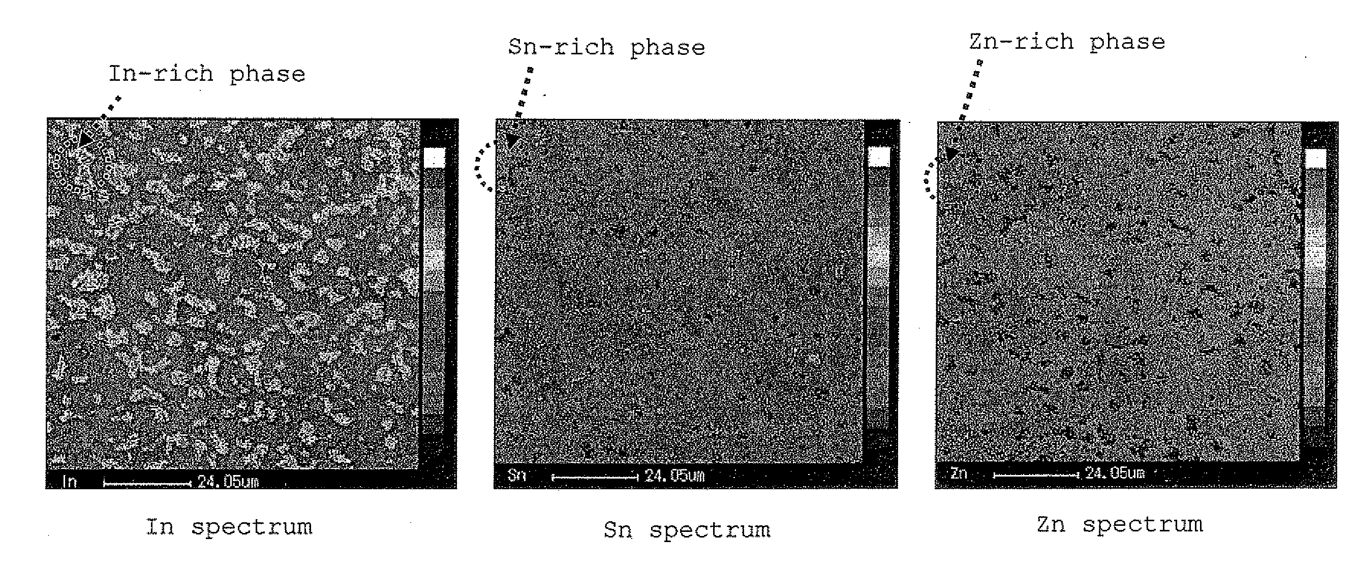
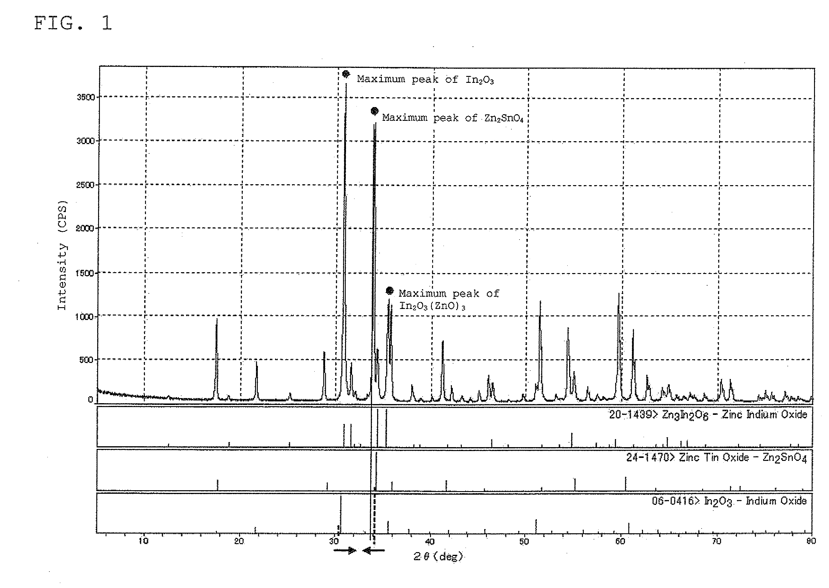
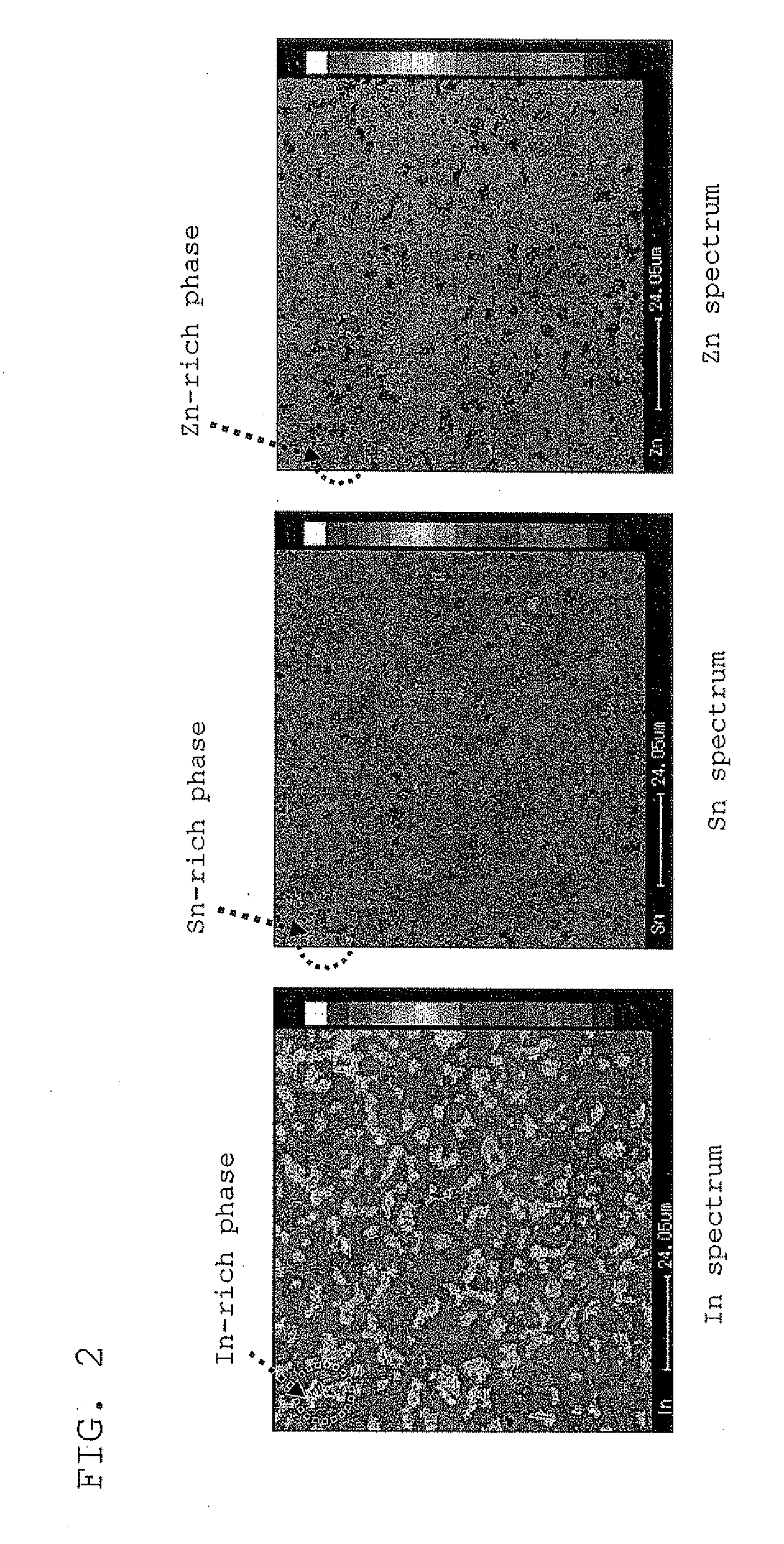
(1) Production of Sputtering Target

[0172]As raw materials for the target, indium oxide with an average particle diameter of 1 μm or less and a purity of 4N, zinc oxide with an average particle diameter of 1 μm or less and a purity of 4N, and tin oxide with an average particle diameter of 1 μm or less and a purity of 4N were mixed at atomic ratios of In / (In+Sn+Zn)=0.44, Sn / (In+Sn+Zn)=0.12, and Zn / (In+Sn+Zn)=0.44. The mixture was supplied to a wet-type ball mill and pulverized for 20 hours to obtain a raw material fine powder.

[0173]The resulting mixture slurry was removed, filtered, dried and granulated. The granulated product was then molded by the cold isostatic pressing at a pressure of 294 MPa. The molded product was placed in a firing kiln, and fired at 1400° C. for 48 hours under an oxygen gas pressure, whereby a sintered body (target) was obtained. The heating rate was 50° C. / hour until it reached 1,000° C. Between 1,000° C. and 1,400° C., the heating rate was 150° C. / hour. The...


PUM

PropertyMeasurementUnit
Temperatureaaaaaaaaaa
Fractionaaaaaaaaaa
Timeaaaaaaaaaa

Abstract

A sputtering target including indium, tin, zinc and oxygen, and including a hexagonal layered compound, a spinel structure compound and a bixbyite structure compound.

Description

TECHNICAL FIELD[0001]The present invention relates to a sputtering target prepared by sintering (hereinafter often referred to as sputtering target or simply as target), a transparent conductive film formed by using a sputtering target, and a transparent electrode.BACKGROUND[0002]In recent years, development of displays has been remarkable. Liquid crystal displays (LCD), electroluminescence displays (EL), field emission displays (FED), or the like are used as display devices for business machines such as personal computers and word processors, and control systems in factories. These displays have a sandwich structure in which a display device is held between transparent conductive oxides.[0003]A mainstream material for such a transparent conductive oxide is indium tin oxide (hereinafter occasionally abbreviated as “ITO”) prepared by a sputtering method, an ion plating method, or a vapor deposition method as described in Non-Patent Document 1.[0004]ITO is composed of a specific amoun...

Claims


Application Information

Patent Timeline
IPC IPC(8): H01B1/02C23C14/34C23F1/16C04B35/64
CPCC04B35/453Y10T428/24777C04B35/6262C04B2235/3284C04B2235/3286C04B2235/3293C04B2235/5445C04B2235/6562C04B2235/6565C04B2235/6567C04B2235/6585C04B2235/664C04B2235/763C04B2235/77C04B2235/80C04B2235/963C23C14/086C23C14/3414C04B35/457H01B1/08B22F3/03
Inventor YANO, KOKIINOUE, KAZUYOSHITANAKA, NOBUOTANAKA, TOKIE
Owner IDEMITSU KOSAN CO LTD
Why Eureka
Try Eureka