Method for enhancing electrical injection efficiency and light extraction efficiency of light-emitting devices

a technology of light-emitting devices and efficiency enhancement, which is applied in the direction of semiconductor/solid-state device manufacturing, semiconductor devices, electrical equipment, etc., can solve the problems of current crowding phenomenon, serious total internal reflection and re-absorption phenomena of gan-based light-emitting devices, and low light extraction efficiency of gallium nitride light-emitting devices. achieve the effect of enhancing the efficiency of electrical injection and light extraction efficiency of a light-

Inactive Publication Date: 2011-06-02
WALSIN LIHWA
View PDF20 Cites 19 Cited by
  • Summary
  • Abstract
  • Description
  • Claims
  • Application Information

AI Technical Summary

Benefits of technology

[0009]Accordingly, it is an object of the present invention to provide a method for enhancing electrical injection efficiency and light extraction efficiency of a light-emitting device by forming a window layer with a controllable light escape angle on the light-emitting device.
[0010]In accordance with an aspect of the present invention, a method for enhancing electrical injection efficiency and light extraction efficiency of a light-emitting device includes the steps of: providing a site layer on the light-emitting device; placing a protection layer on the site layer; forming a cavity through the protection layer and the site layer; and growing a window layer in the cavity. The shape of the window layer can be well controlled by adjusting reactive temperature, reactive time, and N2 / H2 concentration ratio of atmosphere such that light escape angle of the window layer can be changed. Otherwise, the surface of window layer can also be roughening with regular or irregular patterns by wet or dry etching processes.
[0021]In accordance with an aspect of the present invention, a method for enhancing electrical injection efficiency and light extraction efficiency of a light-emitting device includes the steps of: a light-emitting substrate; a site layer provided on the light-emitting substrate; a cavity formed through the site layer; a protection layer placed on the site layer having the cavity exposed; and a window layer formed in the cavity. The shape of the window layer can be well controlled by adjusting reactive temperature, reactive time, and N2 / H2 concentration ratio of atmosphere such that light escape angle of the window layer can be changed. Otherwise, the surface of window layer can also be roughening with regular or irregular patterns by wet or dry etching processes.

Problems solved by technology

Gallium nitride (GaN) light-emitting devices have low light extraction efficiency due to large refraction index difference between GaN and air.
Therefore, a serious total internal reflection and re-absorption phenomena would be happened in the GaN-based light-emitting devices.
It is well known that a typical p-type GaN (from 300 to 5000 Å thick) layer has a low current conductivity and poor current spreading ability which might cause current crowding phenomenon due to the acceptor (magnesium, Mg) in the GaN crystal having poor activated ability.
According to those properties, the insulating sapphire substrate can not be a good window layer since the GaN-based LED structure grown on sapphire substrate is a horizontal device, which will decrease its emission efficacy.
Further since such favored paths fall under the opaque electrode, the generated light reaching the electrode is lost.
It might degrade the optical performance of the LEDs due to the input power consumption.
A disadvantage of this arrangement is that the current spreading layer has to be very thick (up to 50 μm) in order for the current to spread out sufficiently as it flows vertically through the wafer.
Such thick layers of bulk semiconductor material are difficult, expensive and time consuming to grow.
Hence, high-intensity LEDs are unreliable owing to threading dislocations and stacking faults which occur near the lattice mismatched AlGaInP and GaP crystal interface, as a result of strain-relaxation in the thick layer.

Method used


Image

  • Method for enhancing electrical injection efficiency and light extraction efficiency of light-emitting devices
  • Method for enhancing electrical injection efficiency and light extraction efficiency of light-emitting devices
  • Method for enhancing electrical injection efficiency and light extraction efficiency of light-emitting devices

Examples


Embodiment Construction

[0041]The present invention will now be described more specifically with reference to the following embodiment. It is to be noted that the following descriptions of preferred embodiment of this invention are presented herein for purpose of illustration and description only; it is not intended to be exhaustive or to be limited to the precise form disclosed.

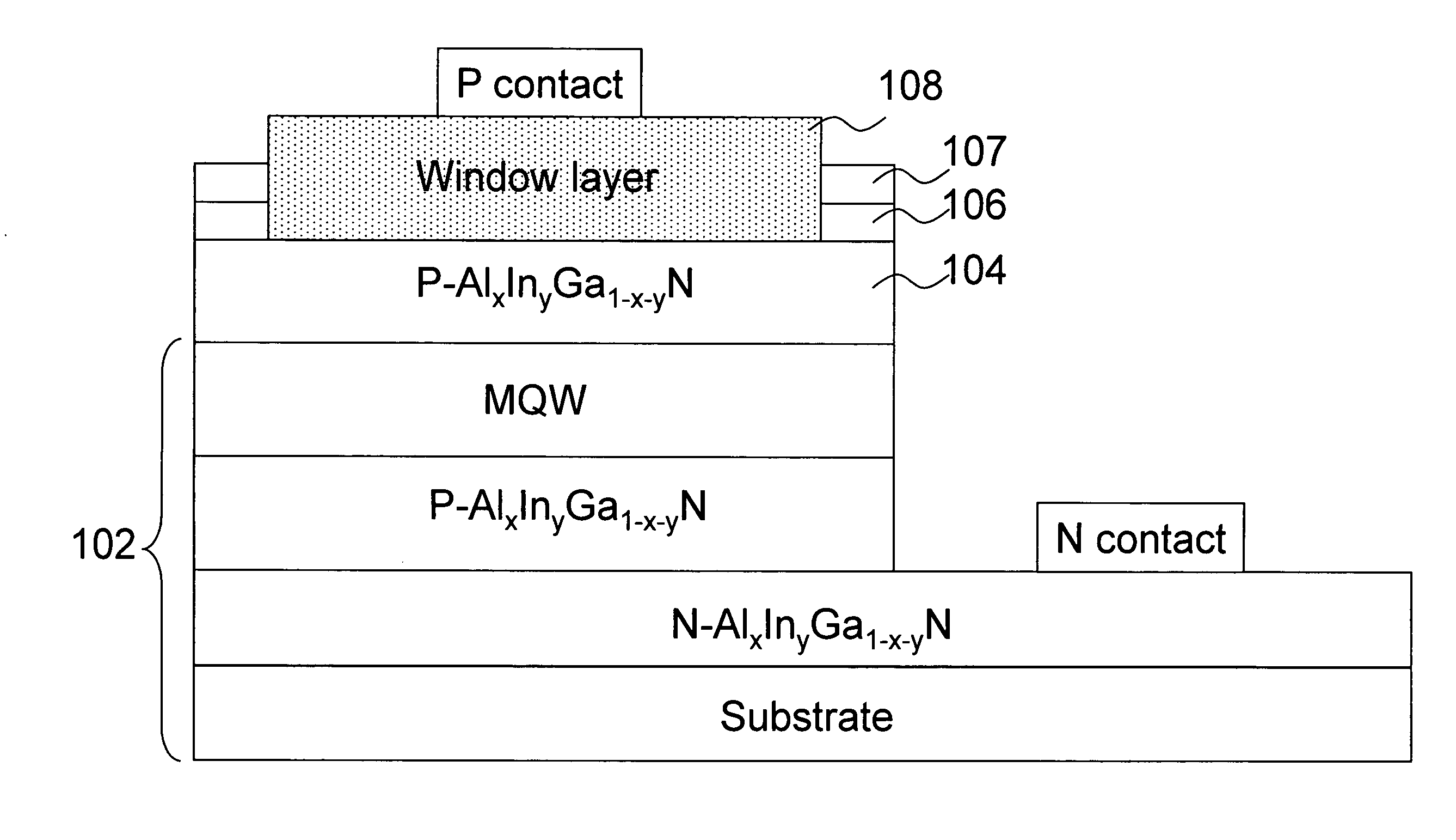
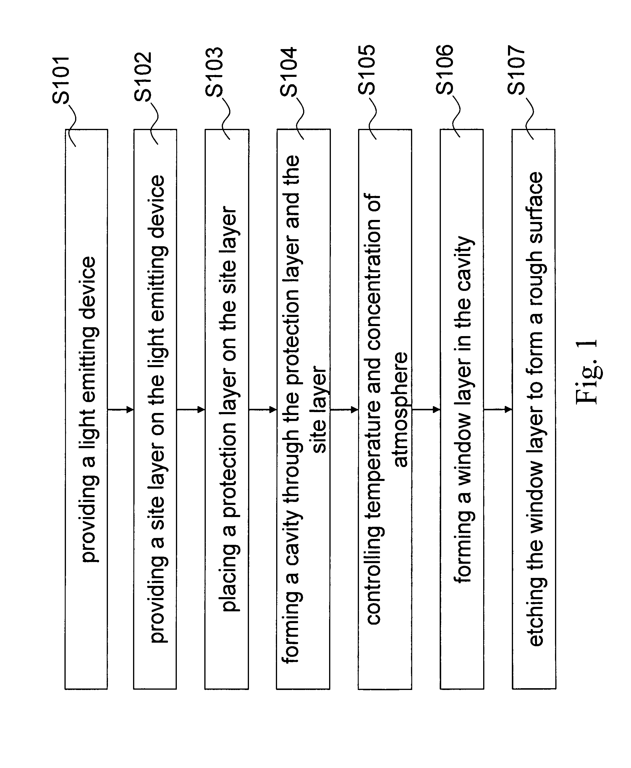
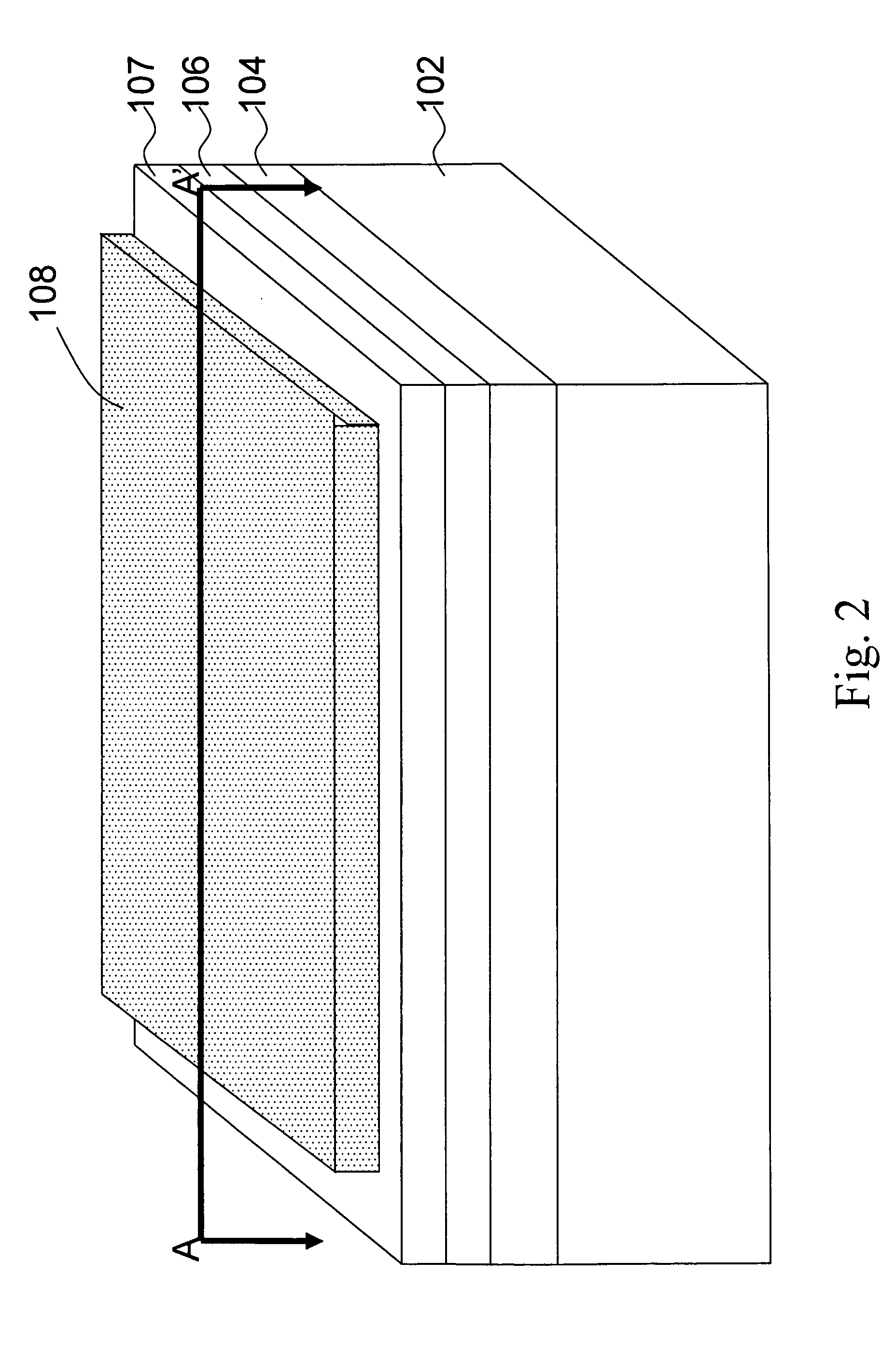
[0042]FIG. 1 is a flow chart of a preferred embodiment according to the present invention showing a method for enhancing electrical injection efficiency and light extraction efficiency of a light-emitting device by forming a window layer with a controllable light escape angle on a light-emitting device. FIG. 2 is a three dimensional view of the present invention. It also shows the relative position for each element in the present invention. Now, please refer to FIGS. 1 and 2. The method of the present invention for enhancing electrical injection efficiency and light extraction efficiency of a light-emitting device by forming a wind...


PUM

PropertyMeasurementUnit
thicknessaaaaaaaaaa
reactive temperatureaaaaaaaaaa
thickaaaaaaaaaa

Abstract

A method for enhancing electrical injection efficiency and light extraction efficiency of a light-emitting device is disclosed. The method includes the steps of: providing a site layer on the light-emitting device; placing a protection layer on the site layer; forming a cavity through the protection layer and the site layer; and growing a window layer in the cavity. The shape of the window layer can be well controlled by adjusting reactive temperature, reactive time, and N2 / H2 concentration ratio of atmosphere such that light escape angle of the window layer can be changed.

Description

FIELD OF THE INVENTION[0001]The present invention relates to a method for enhancing electrical injection efficiency and light extraction efficiency of a light-emitting device. More particularly, the present invention relates to a method for preventing current crowding phenomenon, enhancing electrical injection efficiency and light extraction efficiency of a light-emitting device by forming a zinc oxide window layer on the light-emitting device.BACKGROUND OF THE INVENTION[0002]Gallium nitride (GaN) light-emitting devices have low light extraction efficiency due to large refraction index difference between GaN and air. The light emitted from the active layer in a GaN-based light-emitting device is significantly trapped in the GaN-based layer. Therefore, a serious total internal reflection and re-absorption phenomena would be happened in the GaN-based light-emitting devices. It is well known that a typical p-type GaN (from 300 to 5000 Å thick) layer has a low current conductivity and p...

Claims


Application Information

Patent Timeline
Patent Type & Authority Applications(United States)
IPC IPC(8): H01L33/00
CPCH01L33/22H01L33/46H01L2933/0016H01L29/778H01L2924/13064H01L29/66462H01L33/58
Inventor PAN, CHANG-CHICHANG JEAN, CHING-HWACHEN, JANG-HO
Owner WALSIN LIHWA
Why Eureka
Try Eureka