Stacked oxide material, semiconductor device, and method for manufacturing the semiconductor device

a technology of semiconductor devices and stacked oxides, which is applied in the direction of natural mineral layered products, paper/cardboard containers, instruments, etc., can solve the problems that the semiconductor materials cannot be used for thin film devices or three-dimensional devices, and achieve low power consumption, high field-effect mobility, and low current.

Active Publication Date: 2011-06-02
SEMICON ENERGY LAB CO LTD
View PDF100 Cites 139 Cited by
  • Summary
  • Abstract
  • Description
  • Claims
  • Application Information

AI Technical Summary

Benefits of technology

[0009]One object of an embodiment of the present invention is to provide a transistor having high field-effect mobility and low off current. In addition, one object of an embodiment of the present invention is to obtain a so-called normally-off switching element and provide a semiconductor device with low power consumption. Further, one object of an embodiment of the present invention is to provide a transistor having high transistor performance and high reliability.
[0105]Further, in the transistor formed using the oxide semiconductor layer including the c-axis-aligned crystal layer, the amount of change in the threshold voltage of the transistor before and after a BT test can be suppressed, so that high reliability can be achieved. In addition, in the transistor formed using the oxide semiconductor layer including the c-axis-aligned crystal layer, the amount of change in threshold voltage of the transistor between before and after a BT test in which the transistor is continuously irradiated with light can be reduced. As a result, the transistor with stable electric characteristics can be manufactured.

Problems solved by technology

However, SiC, GaN, and the like need to be subjected to treatment at a temperature higher than or equal to 1500° C. so as to be crystallized and used as a single crystal component; therefore, these semiconductor materials cannot be used for thin film devices or three-dimensional devices.

Method used


Image

  • Stacked oxide material, semiconductor device, and method for manufacturing the semiconductor device
  • Stacked oxide material, semiconductor device, and method for manufacturing the semiconductor device
  • Stacked oxide material, semiconductor device, and method for manufacturing the semiconductor device

Examples


embodiment 1

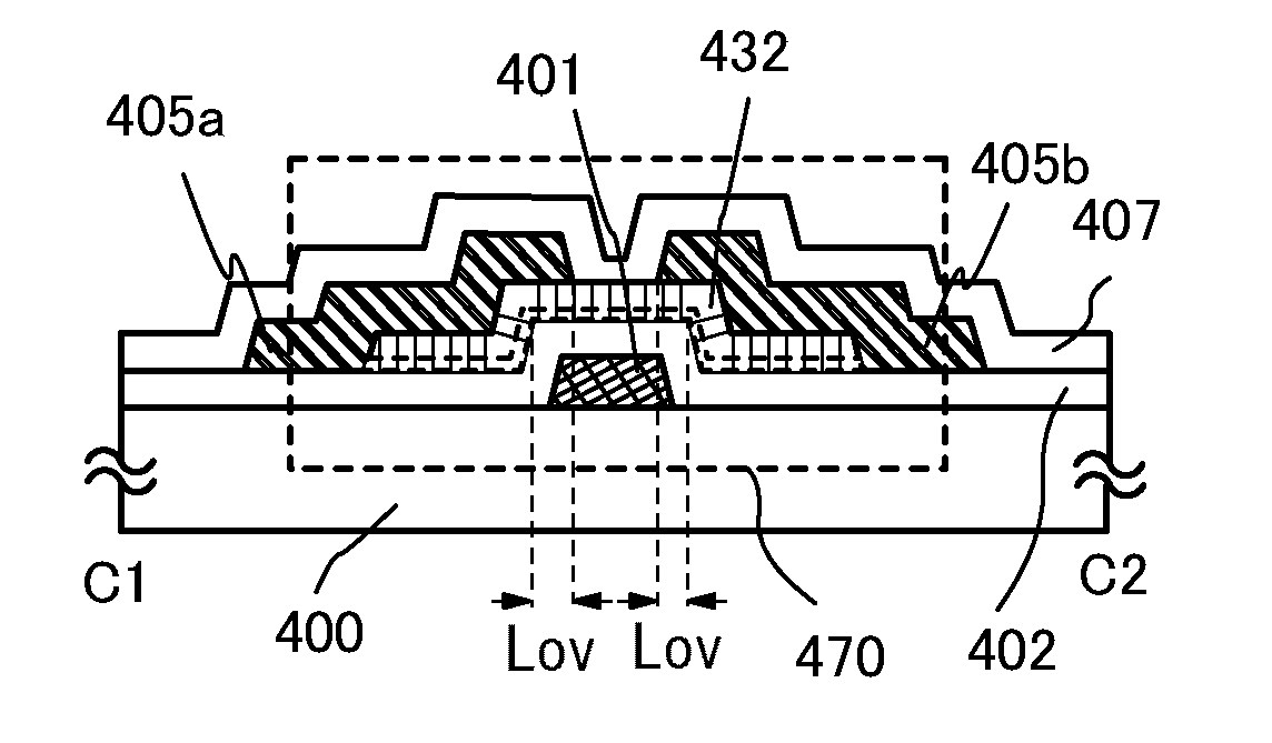
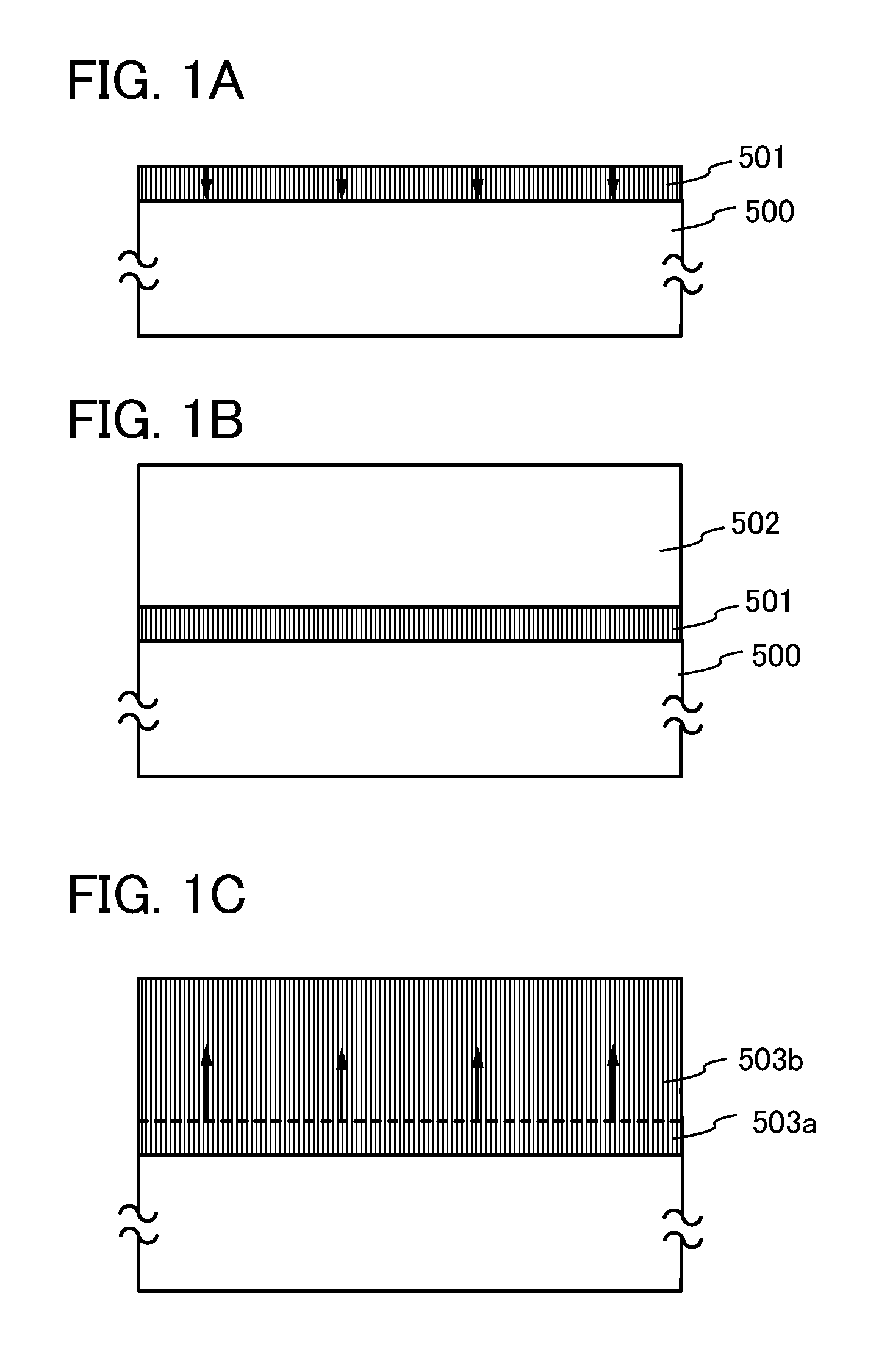
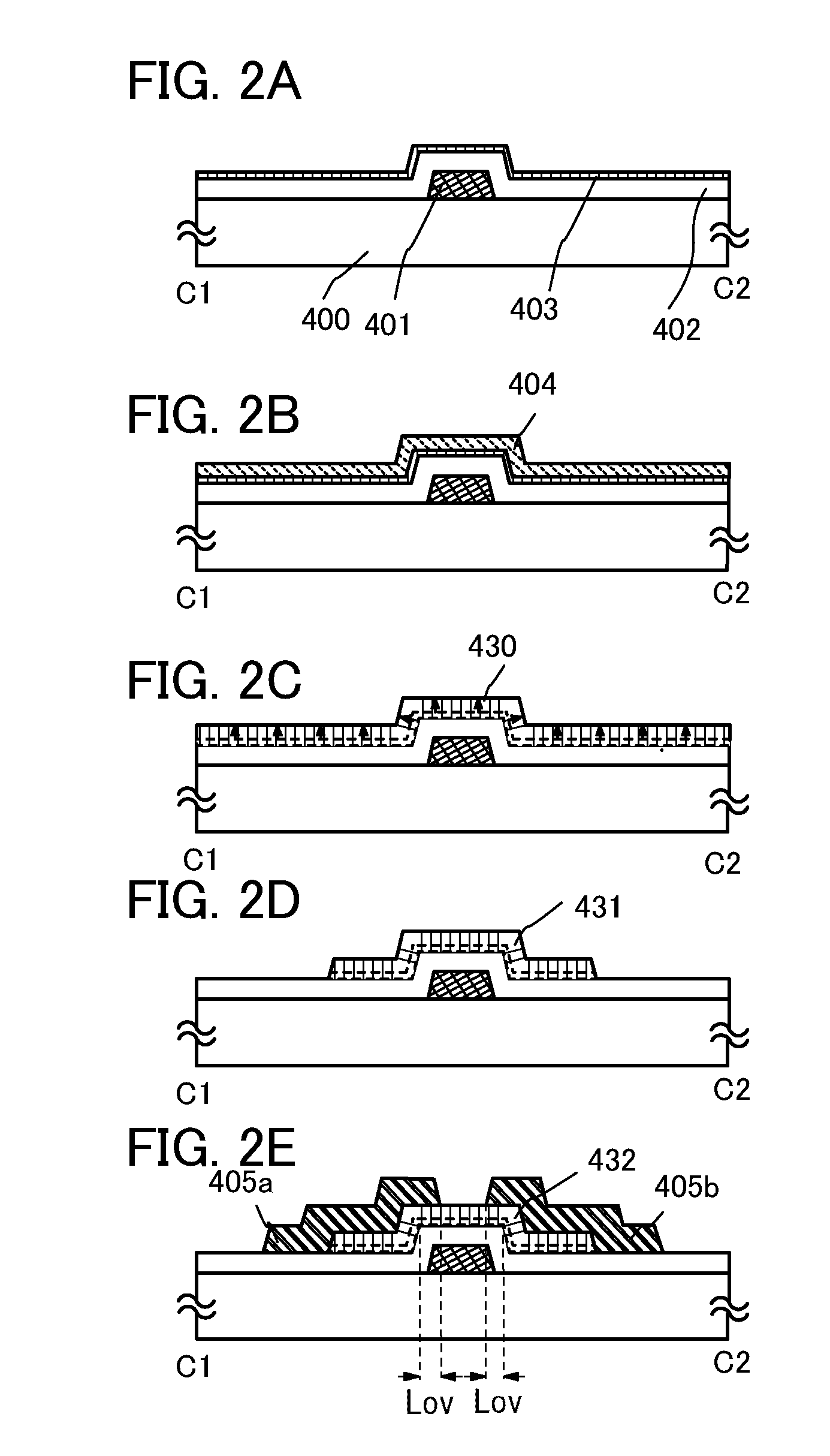
[0123]In this embodiment, an example of manufacturing a transistor is described with reference to FIGS. 1A to 1C, FIGS. 2A to 2E, and FIGS. 3A and 3B.

[0124]First, a conductive film is formed over a substrate 400 which is a substrate having an insulating surface, and then a gate electrode layer 401 is provided using a photolithography step with the use of a photomask.

[0125]As the substrate 400, although a semiconductor substrate, a sapphire substrate, a quartz substrate, a ceramic substrate, and the like are given, a glass substrate which enables mass production is preferably used, in particular. As a glass substrate used for the substrate 400, a glass substrate whose strain point is higher than or equal to 730° C. may be used when the temperature of the heat treatment to be performed is high. For the substrate 400, for example, a glass material such as aluminosilicate glass, aluminoborosilicate glass, or barium borosilicate glass is used. Note that by containing a larger amount of b...

embodiment 2

[0193]In this embodiment, the case where a first oxide component and a second oxide component are formed using oxide semiconductor materials including different components is described, although the case where the first oxide component and the second oxide component are formed using oxide semiconductor materials including the same components is described in Embodiment 1. Note that in FIG. 10A, the same portions as those in FIG. 1A are denoted by the same reference numerals.

[0194]In this embodiment, a first oxide semiconductor layer is formed to a thickness of 5 nm using a metal oxide target which does not include Ga and includes In2O3 and ZnO at 1:2 [molar ratio]. In the case of a bottom-gate transistor, because oxide of Ga is an insulator, higher field-effect mobility is obtained in the case where an In—Zn—O film is used as the first oxide semiconductor layer than in the case where an In—Ga—Zn—O film is used for the first oxide semiconductor layer.

[0195]Next, first heat treatment i...

embodiment 3

[0205]In this embodiment, a transistor including a stacked oxide material including a c-axis-aligned crystal layer is manufactured, and by using the transistor for a pixel portion, and further a driver circuit, a semiconductor device having a display function (also referred to as a display device) is manufactured. Furthermore, when part or whole of a driver circuit using the transistors is formed over the same substrate as a pixel portion, a system-on-panel can be obtained.

[0206]The display device includes a display element. As the display element, a liquid crystal element (also referred to as a liquid crystal display element) or a light-emitting element (also referred to as a light-emitting display element) can be used. The light-emitting element includes, in its category, an element whose luminance is controlled by a current or a voltage, and specifically includes, in its category, an inorganic electroluminescent (EL) element, an organic EL element, and the like. Furthermore, a di...


PUM

PropertyMeasurementUnit
thicknessaaaaaaaaaa
temperatureaaaaaaaaaa

Abstract

One embodiment is a method for manufacturing a stacked oxide material, including the steps of forming a first oxide component over a base component, causing crystal growth which proceeds from a surface toward an inside of the first oxide component by first heat treatment to form a first oxide crystal component at least partly in contact with the base component, forming a second oxide component over the first oxide crystal component; and causing crystal growth by second heat treatment using the first oxide crystal component as a seed to form a second oxide crystal component.

Description

TECHNICAL FIELD[0001]The present invention relates to a stacked oxide material which is formed by stacking films by a sputtering method and the films are subjected to crystallization heat treatment, and which is used for manufacturing a semiconductor device. For example, a material which is suitably used for a semiconductor included in a transistor, a diode, or the like is provided. In addition, the present invention relates to a semiconductor device including a circuit formed with semiconductor elements such as a transistor, and a manufacturing method thereof. For example, the present invention relates to a power device which is mounted on a power supply circuit; a semiconductor integrated circuit including a memory, a thyristor, a converter, image sensor, or the like; and an electronic appliance on which an electro-optical device typified by a liquid crystal display panel or a light-emitting display device including an organic light-emitting element is mounted as a component.[0002...

Claims


Application Information

Patent Timeline
Patent Type & Authority Applications(United States)
IPC IPC(8): H01L29/786B05D3/00B32B37/02C23C14/34B32B9/00H01L21/44
CPCH01L21/02472H01L21/02483H01L21/02554H01L21/02565H01L21/02631H01L27/1225Y10T156/10H01L29/7869H01L29/66969H01L21/16H01L29/66765Y10T428/265H01L29/78609Y10T428/31678
Inventor YAMAZAKI, SHUNPEI
Owner SEMICON ENERGY LAB CO LTD
Why Eureka
Try Eureka