Transparent electroconductive film for solar cell, composition for transparent electroconductive film and multi-junction solar cell

Inactive Publication Date: 2011-06-16
MITSUBISHI MATERIALS CORP
View PDF6 Cites 8 Cited by
  • Summary
  • Abstract
  • Description
  • Claims
  • Application Information

AI Technical Summary

Benefits of technology

[0038]The present invention enables the production of a transparent electroconductive film by a wet coating method using a coating material that satisfies each of the requirements of favorable phototransmittance, high electrical conductivity, low refractive index and the like required when using in a multi-junction solar cell. Moreover, the present invention offers the advantage of being able to reduce running costs during production of a transparent electroconductive film by using a process that does not use vacuum deposition.
[0039]In addition, the present invention offers an additional advantage of being able to optimize light reflection properties between ph

Problems solved by technology

However, the silicon crystals used in bulk solar cells required considerable time and energy to grow the crystals and a complicated process was required in the

Method used


Image

  • Transparent electroconductive film for solar cell, composition for transparent electroconductive film and multi-junction solar cell
  • Transparent electroconductive film for solar cell, composition for transparent electroconductive film and multi-junction solar cell
  • Transparent electroconductive film for solar cell, composition for transparent electroconductive film and multi-junction solar cell

Examples


Example

Example 1

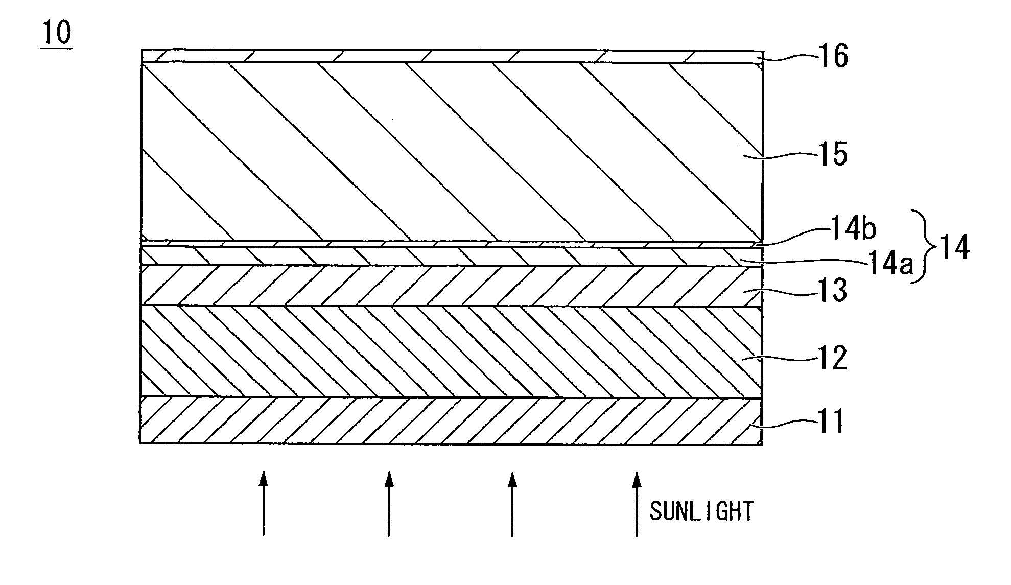
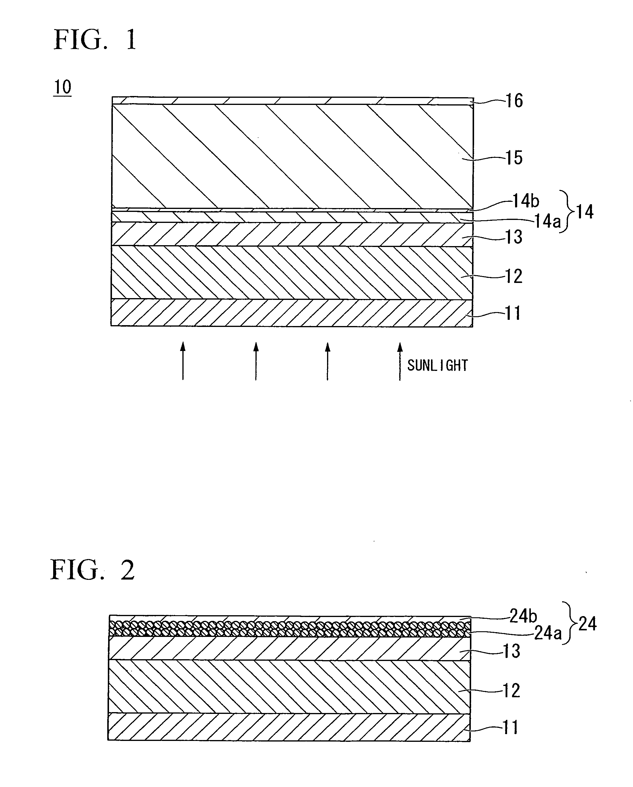
[0090]First, a square piece of glass measuring 10 cm on a side was prepared for the transparent substrate 11, and SnO2 was used for the front side electrode layer 12. The film thickness of the front side electrode layer 12 at this time was 800 nm, the sheet resistance was 10Ω / □, and the haze rate was 15 to 20%. Next, the amorphous silicon layer 13 was deposited onto the front side electrode layer 12 at a thickness of 300 nm using plasma CVD.

[0091]Next, a composition for a transparent electroconductive film composed of an electroconductive fine particle dispersion and a binder dispersion was prepared in the manner described below.

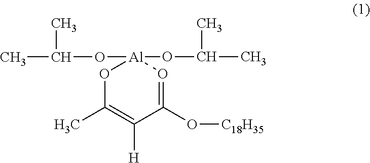
[0092]As shown in Table 1, 1.0 part by weight of ITO powder having an atomic ratio Sn / (Sn+In) of 0.1 and a particle diameter of 0.03 μm was added as electroconductive fine particles, and 0.01 part by weight of the organic titanate coupling agent represented by the aforementioned formula (3) was added as coupling agent followed by the addition of eth...

Example

Example 2

[0101]As shown in Table 1, a multi-junction thin film silicon solar cell was produced and evaluated in the same manner as Example 1 with the exception of using an electroconductive fine particle dispersion obtained by adding 0.5 parts by weight of ITO powder having an atomic ratio Sb / (Sb+In) of 0.05 and a particle diameter of 0.02 μm as electroconductive fine particles and adding 0.01 part by weight of the titanate coupling agent represented by the aforementioned formula (3) as coupling agent followed by adding ethanol as dispersion medium to bring to a total of 100 parts by weight, using a binder dispersion obtained by preparing 0.2 parts by weight of a siloxane polymer as a binder and adding ethanol as a dispersion medium to bring to a total of 100 parts by weight, forming a coated film of electroconductive fine particles by coating the electroconductive fine particle dispersion to a film thickness of the fine particle layer of 20 nm by spin coating, and impregnating the ...

Example

Example 3

[0102]As shown in Table 1, a multi-junction thin film silicon solar cell was produced and evaluated in the same manner as Example 1 with the exception of using an electroconductive fine particle dispersion obtained by adding 1.0 part by weight of PTO powder (P-doped SnO2) having an atomic ratio P / (P+Sn) of 0.1 and a particle diameter of 0.02 μm as electroconductive fine particles and adding 0.02 parts by weight of the titanate coupling agent represented by the aforementioned formula (2) as coupling agent followed by adding ethanol as dispersion medium to bring to a total of 100 parts by weight, forming a coated film of electroconductive fine particles by coating the electroconductive fine particle dispersion to a film thickness of the fine particle layer of 70 nm by spin coating, and impregnating a binder dispersion onto the coated film of electroconductive fine particles to a film thickness after baking of 70 nm by spin coating. Furthermore, the ratio of fine particles to ...


PUM

PropertyMeasurementUnit
Temperatureaaaaaaaaaa
Percent by massaaaaaaaaaa
Thicknessaaaaaaaaaa

Abstract

An object of the present invention is to provide a transparent electroconductive film, which in addition to satisfying each of the requirements of favorable phototransmittance, high electrical conductivity, low refractive index and the like required when using in a multi-junction solar cell, enables running costs to be reduced since the transparent electroconductive film is produced without using a vacuum deposition method. The transparent electroconductive film for a solar cell of the present invention is provided between photoelectric conversion layers of a multi-junction solar cell, a coated film of fine particles formed by coating using a wet coating method is baked, the electroconductive component in the base material that composes the electroconductive film is present within the range of 5 to 95% by weight, and the thickness of the electroconductive film is within the range of 5 to 200 nm.

Description

TECHNICAL FIELD[0001]The present invention relates to a transparent electroconductive film for a solar cell that improves cell output by being provided between photoelectric conversion layers in a multi-junction solar cell having improved conversion efficiency by laminating two or more types of photoelectric conversion layers, a composition for that transparent electroconductive film, and a multi-junction solar cell.BACKGROUND ART[0002]Research and development of clean energy are currently proceeding from the standpoint of environmental protection. In particular, solar cells are attracting attention since they use infinitely available sunlight for their energy source and are non-polluting. In the past, bulk solar cells were used for solar power generation by solar cells, and these were used as semiconductors in the form of thick plates obtained by producing bulk crystals of monocrystalline silicon or polycrystalline silicon and then slicing the crystals into thick plates. However, t...

Claims


Application Information

Patent Timeline
IPC IPC(8): H01L31/06B32B3/00H01B1/22H01B1/24H01L31/0687H01L31/078
CPCH01B1/20H01B1/22H01L31/022466H01L31/043H01L31/078H01L31/1884Y02E10/544H01L31/0687H01L31/042Y02E10/548H01L31/03762
Inventor ARAI, MASAHIDEYAMASAKI, KAZUHIKOOGAWA, SATOKOHAYASHI, TOSHIHARU
Owner MITSUBISHI MATERIALS CORP
Why Eureka
Try Eureka