Semiconductor light-emitting devices having concave microstructures providing improved light extraction efficiency and method for producing same

Active Publication Date: 2011-06-30
LEHIGH UNIVERSITY
View PDF12 Cites 25 Cited by
  • Summary
  • Abstract
  • Description
  • Claims
  • Application Information

AI Technical Summary

Benefits of technology

[0008]Yet another approach for significantly enhancing the light extraction efficiency of III-Nitride LEDs involves fabricating SiO2/polystyrene (PS) microlens arrays. This approach is described in detail in U.S. patent application Ser. No. 12/520,619, th

Problems solved by technology

Unfortunately, the refractive index difference of GaN (n=2.5) is relatively large compared to air (n=1).
The large mismatch in refractive indices results in a narrow escape cone of only 23.5° with escape probability of only 4% from the top surface of the LED devices, with the rest of the optical power trapped within the semiconductor.
However, the roughness obtained using these methods varies, thus leading to variation in the light extraction efficiency improvement of the LEDs across the wafer sample.
Similarly, such etching results in a surface of the mesa sidewalls that is non-uniform.
However, the improvement of the light extraction efficiency in LED employing oblique mes

Method used


Image

  • Semiconductor light-emitting devices having concave microstructures providing improved light extraction efficiency and method for producing same
  • Semiconductor light-emitting devices having concave microstructures providing improved light extraction efficiency and method for producing same
  • Semiconductor light-emitting devices having concave microstructures providing improved light extraction efficiency and method for producing same

Examples


examples

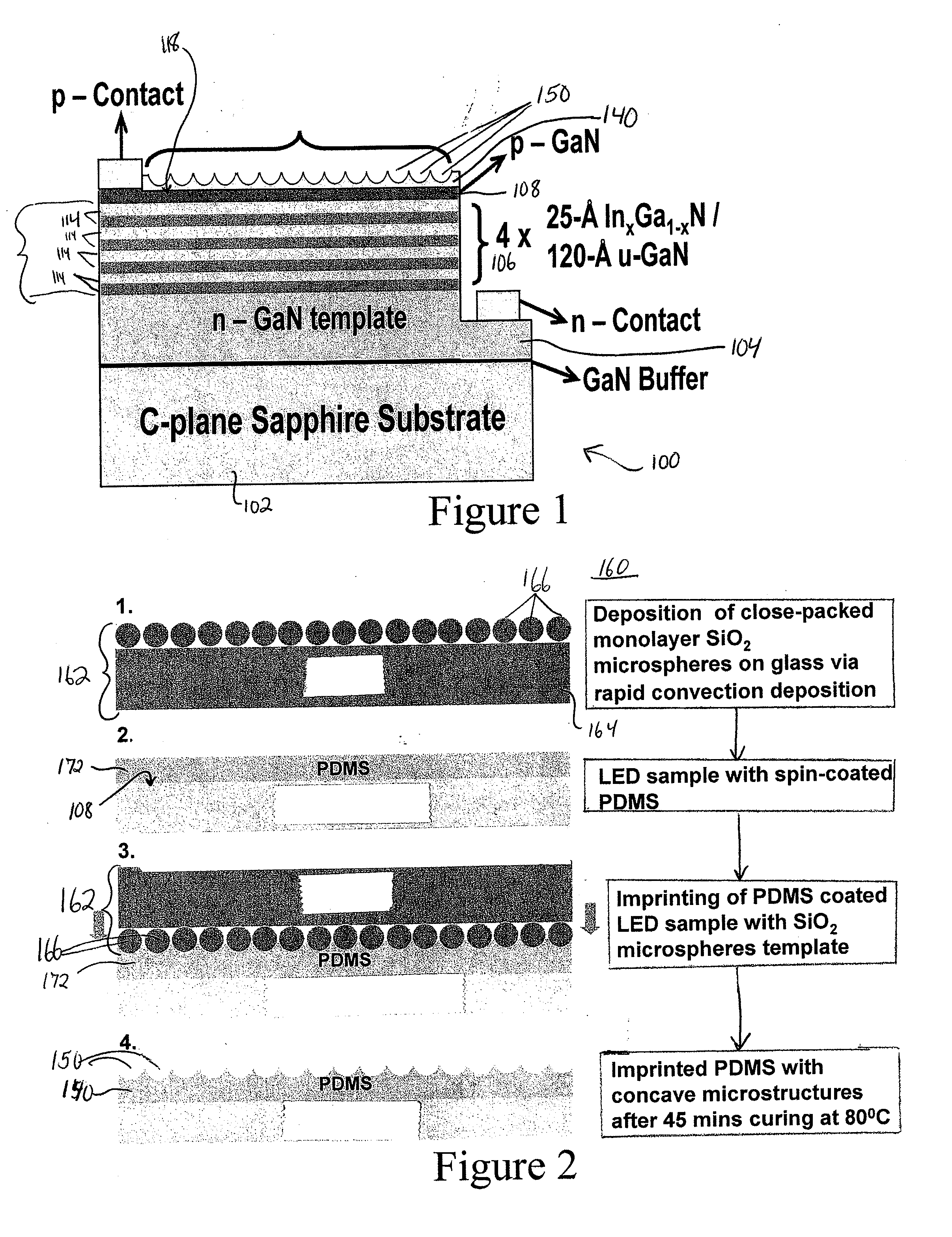
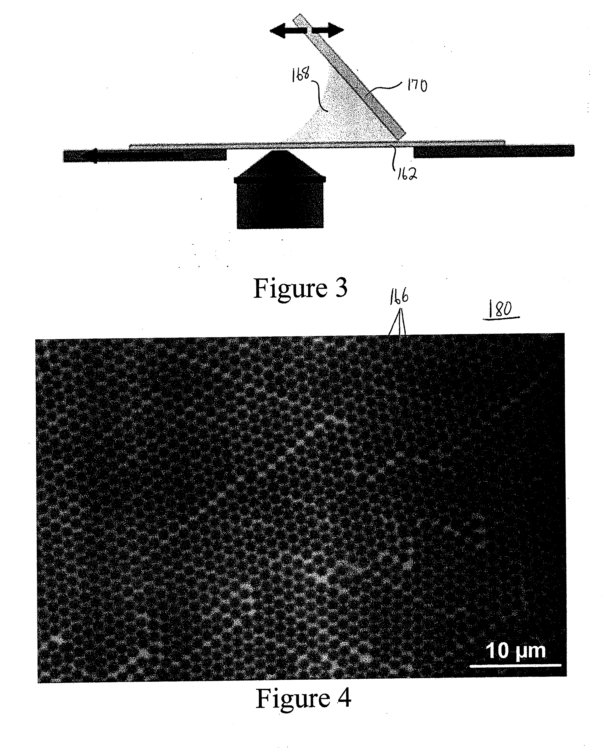
[0048]In these Examples, a monolayer of SiO2 microspheres was first deposited on a glass slide using the low-cost rapid convective deposition technique, consistent with the schematic of the rapid convective deposition technique shown in FIG. 2. The deposition blade 170 and the glass slide 162 forms a wedge-shaped corner. 10 μL of the monosized SiO2 colloidal suspension was injected to a corner between the deposition blade 170 and substrate 162. The deposition blade was then swept across the glass slide with a linear motor. Deposition speed was varied to optimize deposition of a monolayer SiO2 microspheres. A confocal laser scanning micrograph (CLSM) of the monolayer SiO2 microsphere arrays on the glass substrate is shown in FIG. 4.

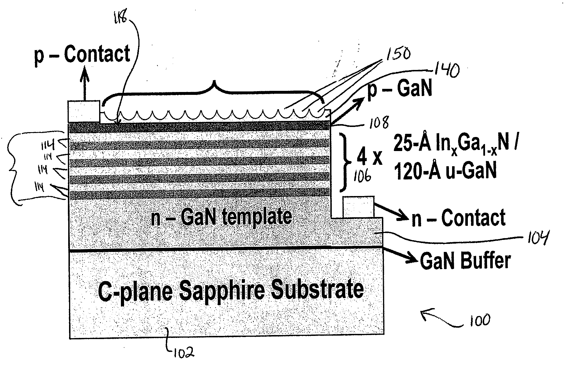
[0049]To form the concave microstructures on top of the LED structure, in this example the LED wafer was pre-patterned with 3.6 μm thick photoresist (PR 1813) to cover the p- and n-metal contacts of the LEDs. The p-metal for the LEDs used in this experimen...


PUM


Abstract

A conventional semiconductor LED is modified to include a microlenslayer over its light-emitting surface. The LED may have an active layer including at least one quantum well layer of InGaN and GaN. The microlens layer includes a plurality of concave microstructures that cause light rays emanating from the LED to diffuse outwardly, leading to an increase in the light extraction efficiency of the LED. The concave microstructures may be arranged in a substantially uniform array, such as a close-packed hexagonal array. The microlens layer is preferably constructed of curable material, such as polydimethylsiloxane (PDMS), and is formed by soft-lithography imprinting by contacting fluid material of the microlens layer with a template bearing a monolayer of homogeneous microsphere crystals, to cause concave impressions, and then curing the material to fix the concave microstructures in the microlens layer and provide relatively uniform surface roughness.

Description

CROSS-REFERENCE TO RELATED APPLICATIONS[0001]This application claims the benefit of priority under 35 U.S.C. §119(e) of U.S. Provisional Patent Application No. 61 / 267,523, filed Dec. 8, 2009, the entire disclosure of which is hereby incorporated herein by reference.STATEMENT REGARDING FEDERALLY-SPONSORED RESEARCH OR DEVELOPMENT[0002]This invention was made with government support under U.S. National Science Foundation—ECCS Award # 0701421, US National Science Foundation—CBET Award # 0828426, and US Department of Energy—NETL (DE-FC26-08NT01581). The government has certain rights in the invention.FIELD OF THE INVENTION[0003]The present invention relates generally to semiconductor light-emitting devices (LEDs), and more particularly to a semiconductor LED having improved light extraction efficiency, and a method for making same.DISCUSSION OF RELATED ART[0004]A semiconductor LED is a semiconductor device that emits incoherent narrow-spectrum light when electrically biased in the forward...

Claims


Application Information

Patent Timeline
IPC IPC(8): H01L33/32H01L33/58H01L33/50
CPCH01L33/06H01L33/22H01L2933/0091H01L2933/0058H01L33/58
Inventor TANSU, NELSONGILCHRIST, JAMES F.EE, YIK-KHOONKUMNORKAEW, PISIST
Owner LEHIGH UNIVERSITY
Why Eureka
Try Eureka