Method for manufacturing group iii nitride semiconductor light emitting element, group iii nitride semiconductor light emitting element and lamp

a technology of nitride and light emitting elements, which is applied in the manufacturing of semiconductor/solid-state devices, semiconductor devices, electrical devices, etc., can solve the problems of difficult epitaxial growth of crystals, large lattice mismatch, and inability to obtain crystals having excellent crystallinity, etc., to achieve excellent crystallinity, excellent emission intensity, and suppressed warping

Active Publication Date: 2011-07-07
TOYODA GOSEI CO LTD
View PDF5 Cites 23 Cited by
  • Summary
  • Abstract
  • Description
  • Claims
  • Application Information

AI Technical Summary

Benefits of technology

[0034]The method for manufacturing a group III nitride semiconductor light emitting element of the present invention is a method wherein a substrate having a diameter of 4 inches (100 mm) or larger, with at least a part of the edge of the substrate having an amount of warping H within a range from 0.1 to 30 μm in the direction of warping toward the principal plane, is prepared; the X-ray rocking curve half width of the (0002) plane is 100 arcsec or less and the X-ray rocking curve half width of the (10-10) plane is 300 arcsec or less, in a state where an intermediate layer has been formed on this substrate and thereafter an underlayer and an n-type contact layer are formed on the intermediate layer; and furthermore an n-type cladding layer, a light emitting layer, a p-type cladding layer, and a p-type contact layer are formed on this n-type contact layer. Therefore, warping can be as suppressed as much as possible after the formation of the intermediate layer, the underlayer, and the n-type contact layer on the substrate, and a semiconductor layer including a light emitting layer of excellent crystallinity can be formed thereon. As a result, a group III nitride semiconductor light emitting element with excellent emission intensity and stable emission wavelength can be obtained.
[0035]Furthermore, the lamp of the present invention uses the group III nitride semiconductor light emitting element of the present invention mentioned above, and therefore has excellent light emission characteristics.

Problems solved by technology

There is a large lattice mismatch between such a different kind of substrate and a group III nitride semiconductor crystal epitaxially grown thereon.
In general, if there is such a large lattice mismatch, there is a problem in that it would be difficult to epitaxially grow the crystal directly on the substrate, and even if it is grown, it would be impossible to obtain a crystal having an excellent crystallinity.
If a light emitting element is produced by laminating a semiconductor layer composed of a group III nitride semiconductor on such a largely warped semiconductor substrate, troubles may occur particularly during the exposure in the photolithographic process, the process to grind the backside of the substrate, or the like.
For example, if the substrate is largely warped during the exposure by using a photolithographic method, the distance between the photomask and the resist becomes uneven in the substrate plane, and the dimensions of the photomask and the substrate are mismatched in the substrate plane, and as a result, there is a problem that the mask alignment can not be precisely done in the entire substrate plane.
However, if the substrate is largely warped, there is a problem that the substrate may be broken during the grinding process.
Furthermore, if the substrate is largely warped at the time of lamination of a semiconductor layer composed of a group III nitride semiconductor, there is a problem that the crystallinity and therefore the light emission characteristics may be deteriorated, because the temperature distribution becomes uneven in the plane, and thus the film thickness and the composition of each layer may become uneven.
However, if the underlayer formed on the substrate is made thin as in Patent Document 5, there is a big problem that the crystallinity of the light emitting layer provided on the semiconductor layer formed thereon is deteriorated, and therefore the light emission output power is also lowered and the emission wavelength becomes uneven.

Method used


Image

  • Method for manufacturing group iii nitride semiconductor light emitting element, group iii nitride semiconductor light emitting element and lamp
  • Method for manufacturing group iii nitride semiconductor light emitting element, group iii nitride semiconductor light emitting element and lamp
  • Method for manufacturing group iii nitride semiconductor light emitting element, group iii nitride semiconductor light emitting element and lamp

Examples


example 1

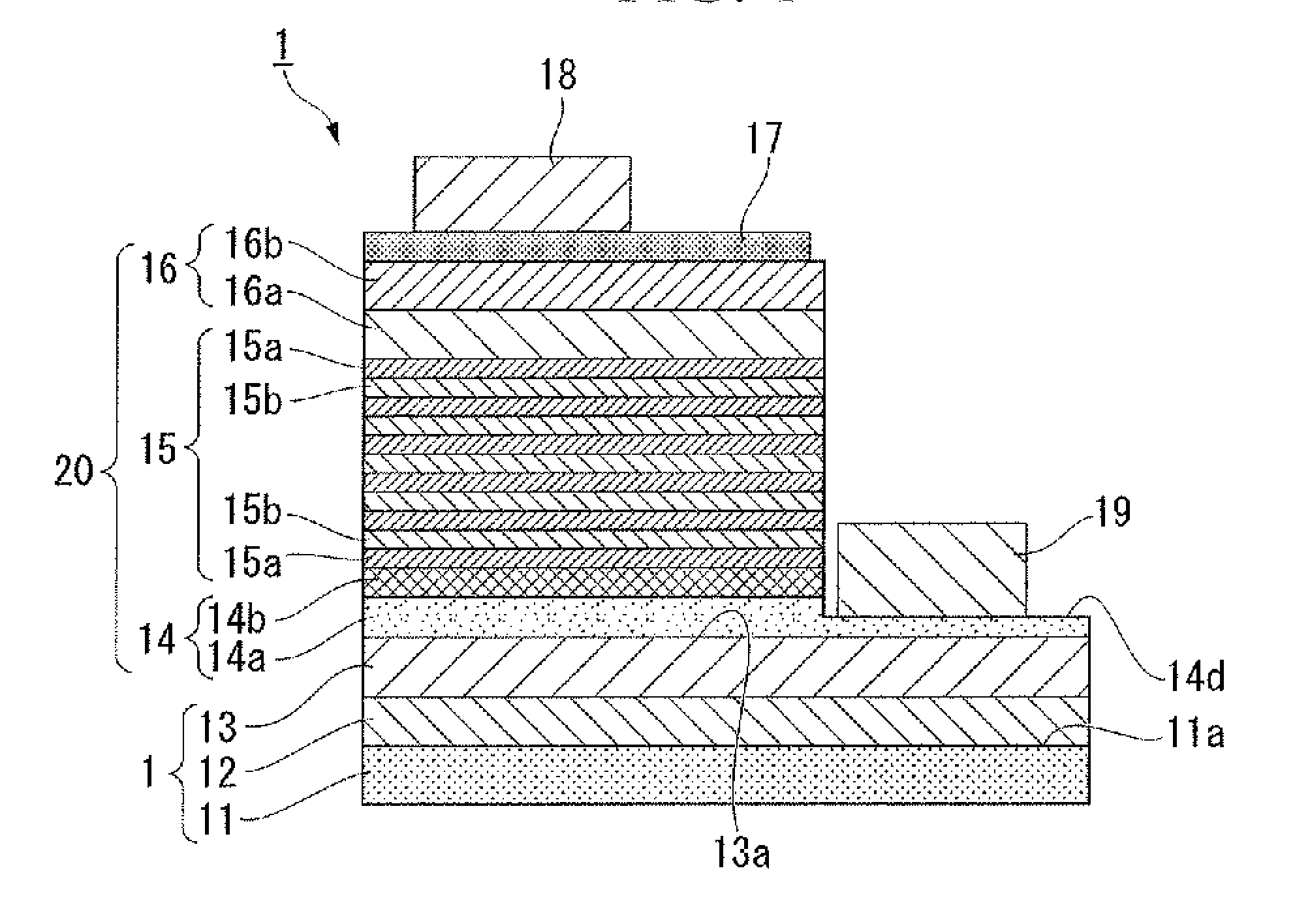
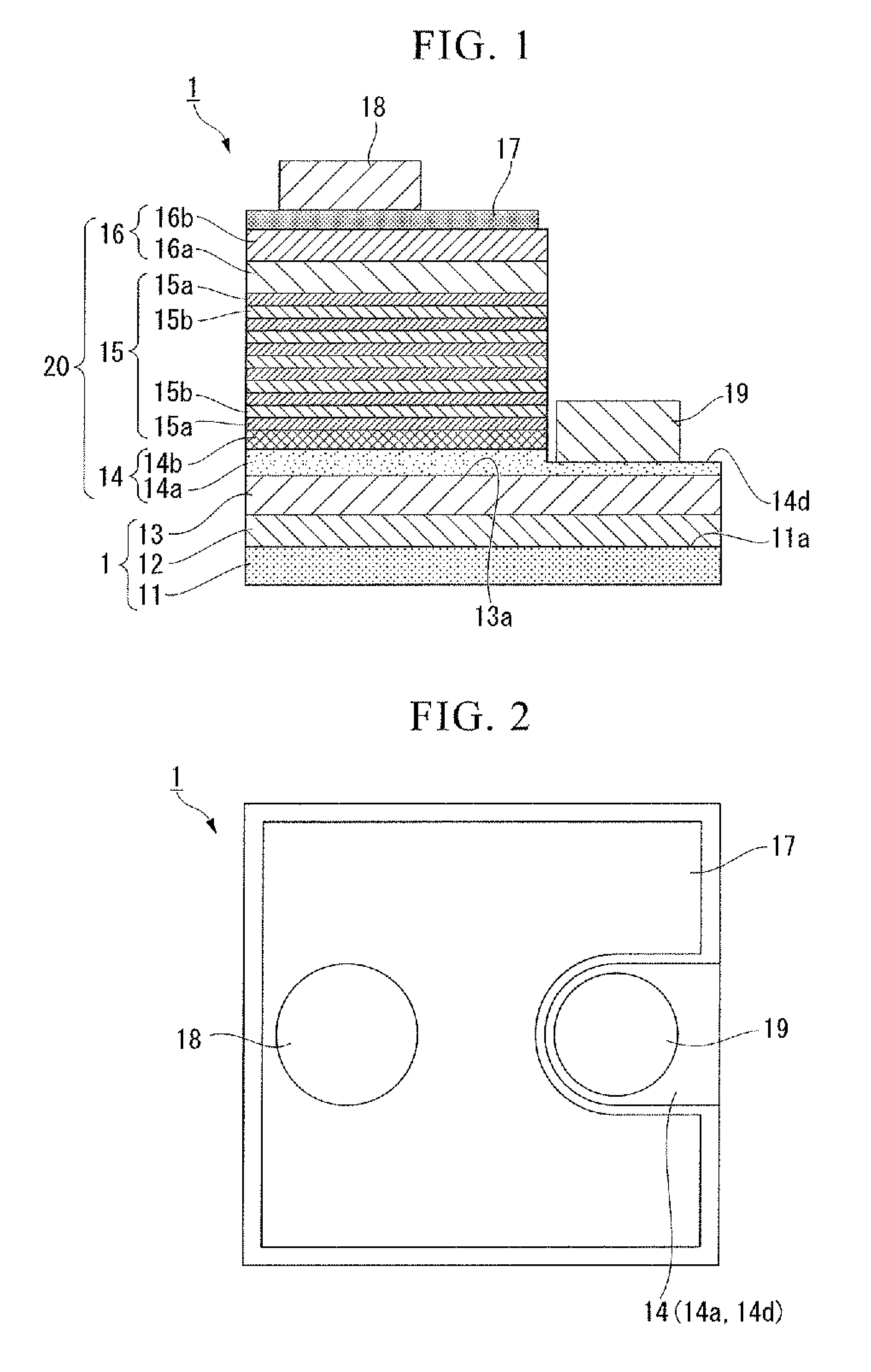
[0190]In this Example, an AlN layer was formed as the intermediate layer 12 by an RF sputtering method on the c-plane (principal plane 11a) of the sapphire substrate 11 having a diameter of 4 inches (100 mm). A GaN layer was formed as the underlayer 13 thereon by an MOCVD method. By so doing, a wafer in which the intermediate layer 12 and the underlayer 13 were deposited on the substrate 11 was produced. Then, further, the semiconductor layer 20 was formed on the underlayer 13, by which the light emitting element 1 as shown in FIG. 1 was produced. Moreover, the lamp 3 (light emitting diode: LED) as shown in FIG. 4 was produced using this light emitting element 1.

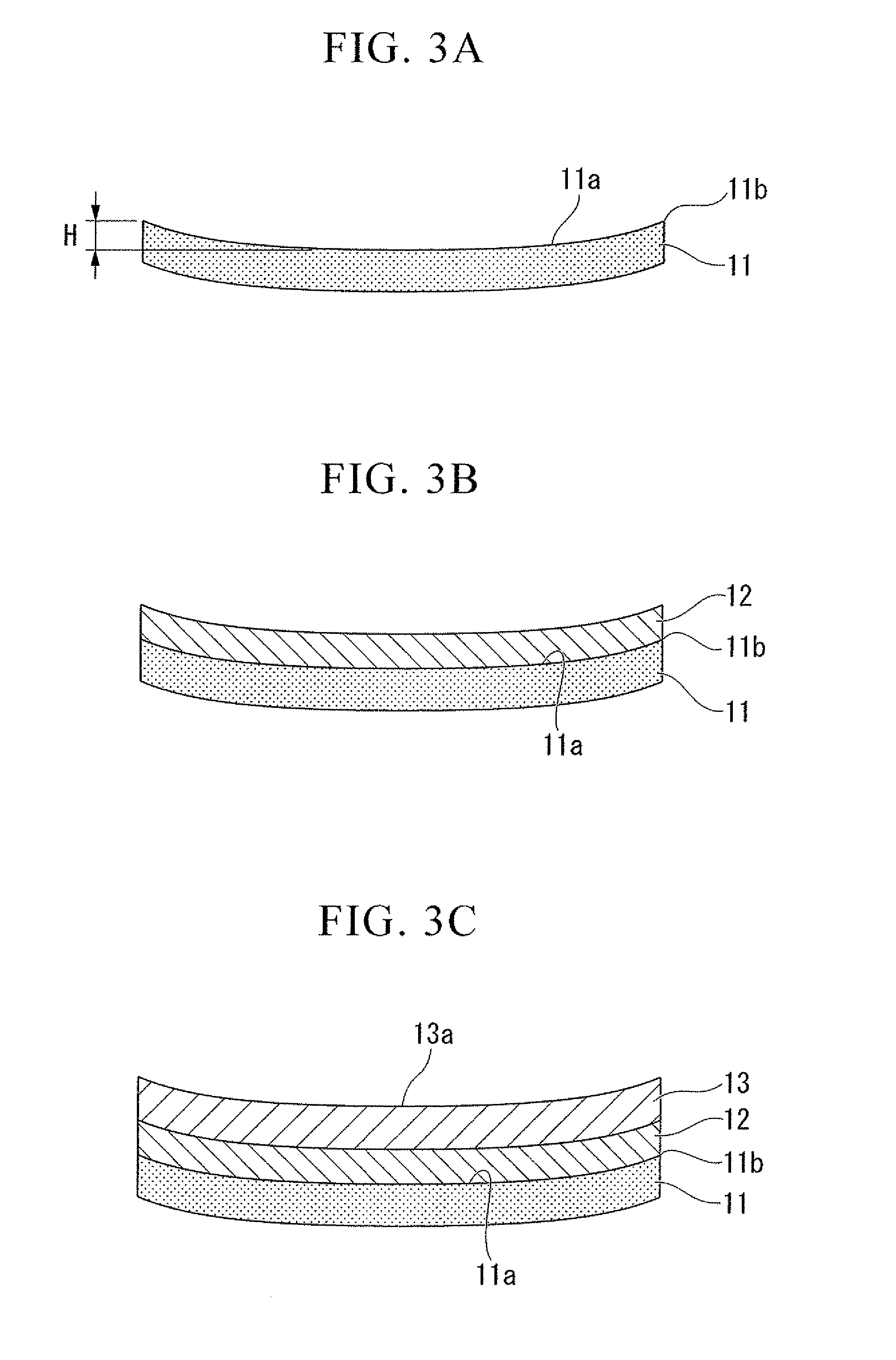
[0191]First, a sapphire substrate 11 having a diameter of 4 inches (101.6 mm; simply expressed as 100 mm in the description of this application) was prepared, and was subjected to both methods of heating and applying a stress so as to adjust the substrate 11 such that at least a part of the substrate edge 11b had an amount o...

example 2

[0227]In the same manner as that of Example 1, a 4-inch (100 mm) sapphire substrate was prepared. A semiconductor light emitting element was formed on this substrate in the same manner as that of Example 1, with the exception that the thickness of the substrate, the amount of warping H (μm) at room temperature, the X-ray rocking curve half width of the (0002) plane (arcsec), and the X-ray rocking curve half width of the (10-10) plane (arcsec) were set at values shown in Table 1. The wavelength distribution σ was evaluated and was shown to be 3.2 nm, being within a preferable range.

example 3

[0228]A 6-inch (150 mm) sapphire substrate was prepared. A semiconductor light emitting element was formed on this substrate in the same manner as that of Example 1, with the exception that the thickness of the substrate, the amount of warping H (μm) at room temperature, the X-ray rocking curve half width of the (0002) plane (arcsec), and the X-ray rocking curve half width of the (10-10) plane (arcsec) were set at values shown in Table 1. The wavelength distribution σ was evaluated and was shown to be 4.4 nm, being within a preferable range.


PUM


Abstract

The present invention provides a method for manufacturing a group III nitride semiconductor light emitting element, with which warping can be suppressed upon the formation of respective layers on the substrate, a semiconductor layer including a light emitting layer of excellent crystallinity can be formed, and excellent light emission characteristics can be obtained; such a group III nitride semiconductor light emitting element; and a lamp. Specifically disclosed is a method for manufacturing a group III nitride semiconductor light emitting element, in which an intermediate layer, an underlayer, an n-type contact layer, an n-type cladding layer, a light emitting layer, a p-type cladding layer, and a p-type contact layer are laminated in sequence on a principal plane of a substrate, wherein a substrate having a diameter of 4 inches (100 mm) or larger, with having an amount of warping H within a range from 0.1 to 30 μm and at least a part of the edge of the substrate warping toward the principal plane at room temperature, is prepared as the substrate; the X-ray rocking curve full width at half maximum (FWHM) of the (0002) plane is 100 arcsec or less and the X-ray rocking curve FWHM of the (10-10) plane is 300 arcsec or less, in a state where the intermediate layer has been formed on the substrate and where thereafter the underlayer and the n-type contact layer are formed on the intermediate layer; and furthermore the n-type cladding layer, the light emitting layer, the p-type cladding layer, and the p-type contact layer are formed on the n-type contact layer.

Description

TECHNICAL FIELD[0001]The present invention relates to a method for manufacturing a group III nitride semiconductor light emitting element, a group III nitride semiconductor light emitting element produced by this method, and a lamp using the same.[0002]Priority is claimed on Japanese Patent Application No. 2008-237209, filed Sep. 16, 2008, the content of which is incorporated herein by reference.BACKGROUND ART[0003]Group III nitride semiconductors have a direct transition-type band-gap in an energy range from visible light to ultraviolet light and exhibit an excellent light emission efficiency, and thus group III nitride semiconductors have been manufactured as semiconductor light emitting elements such as a light emitting diode (LED) and a laser diode (LD) for use in various applications. Even when used in an electronic device, group III nitride semiconductors have a potential to provide better properties than cases where conventional types of group III-V compound semiconductors ar...

Claims


Application Information

Patent Timeline
Patent Type & Authority Applications(United States)
IPC IPC(8): H01L33/30H01L33/36
CPCH01L21/0237H01L21/0242H01L21/02458H01L21/0254H01L33/007H01L21/02609H01L21/0262H01L21/02631H01L21/02573H01L2224/32257H01L2224/32245H01L2224/48091H01L2224/48247H01L2224/48257H01L2224/49107H01L2224/73265H01L2224/45144H01L2924/181H01L2924/00014H01L2924/00H01L2924/00012H01L33/16
Inventor SAKAI, HIROMITSUHARADA, TAKESHI
Owner TOYODA GOSEI CO LTD
Why Eureka
Try Eureka