Forming ii-vi core-shell semiconductor nanowires

a technology of semiconductor nanowires and core shells, which is applied in the field of forming low defect iivi coreshell semiconductor nanowires, can solve the problems of poor color, high cost, and sub-desirable efficiency, and achieve the effects of reducing melting point, low cost, and few unwanted native defects

Inactive Publication Date: 2011-07-21
NANOCO TECH LTD
View PDF7 Cites 27 Cited by
  • Summary
  • Abstract
  • Description
  • Claims
  • Application Information

AI Technical Summary

Benefits of technology

[0015]It is an advantage of the present invention to enable the formation of high quality II-VI core-shell semiconductor nanowires which contain few unwanted native defects. By employing gold-tin alloys as the metal catalysts in the VLS growth of II-VI core-shell semiconductor nanowires, the catalysts have a much reduced melting point which enables the growth temperature of the II-VI core semiconductor nanowires to be lowered to the low 300° C. range. Conventional VLS growth of II-VI semiconductor nanowires using gold catalyst typically involves growth temperatures in the 550° C. range. As is well known in the art, the desired growth temperature for crystalline II-VI semiconductor is in the high 200° C. to low 300° C. temperature range. In this temperature range the number of unwanted native defects is minimized. To turn off the selective localized growth of the nanowires and begin the formation of high quality crystalline shell(s) surrounding the core nanowires, the growth conditions need to be modified. Two approaches are increasing the growth rate by adjusting the precursor flow rates while maintaining the growth temperature in the low 300° C. range; and, the other is increasing the growth temperature to the upper 300° C. range, while maintaining the core precursor flow rates. Combining metal alloy catalysts with the shelling of the core nanowires, results in the formation of the high quality II-VI nanowires. Overall the II-VI core-shell semiconductor nanowires are desirable elements in numerous optoelectronic, electronic, and optical applications, such as, LEDs, lasers, rectifiers, solar cells, transistors, or phosphors.

Problems solved by technology

Despite large gains in their efficiency, OLED lighting will likely remain a niche application due to their environmental sensitivity, shorter lifetime, and low output power density.
The latter issue is the dominant one since it requires OLED lighting products to have large surface areas in order to produce acceptable amounts of lumens.
In spite of the deepening penetration of inorganic LEDs into mainstream lighting, unresolved issues still remain, such as, high cost, poor color, and sub-desirable efficiency.
This “green gap” issue has been recognized for many years (large strain develops in the active region as a result of incorporating sufficient In in the GaN in order to form green emitting InGaN) and despite numerous efforts, still remains largely unresolved.
Unfortunately, the correlated color temperature (CCT) of the corresponding white is typically high (>6000 K), yielding a cold light which lacks sufficient red response.
Another outstanding issue is the efficiency of the phosphors, which for commercial phosphors are currently at 65% (include the efficiency hit due to the Stoke shift) (D. Haranath et al., Appl. Phys. Lett. 89, 173118 (2006)).
Both inorganic LED approaches for white light, as of today, are approximately a factor of 100 too costly to engender significant market penetration into the residential market without significant government subsidies or incentives.
As discussed above, despite the impressive efficiency and large penetration to date of inorganic LEDs (to be called LEDs) into lighting applications, outstanding issues still remain.
Focusing on color-mixed LEDs (combining red, green, and blue LEDs), the two pressing issues are high cost and the sub-par performance of green LEDs.
A large part of the high cost is associated with conventional LEDs being grown on crystalline substrates.
As discussed above, the sticking point associated with creating efficient InGaN-based LEDs is that incorporating In into the active region results in significant strain relative to the cladding layers (W. Lee et al., J. Display Technol.
Progress has been made on both fronts, but many issues still remain unresolved.
For GaN-based nanowires, efficient doping is still problematic and the quantum efficiency of the emitters remains sub-par (S. Hersee et al., Nano Lett.
For II-VI material based pin nanowires, green LEDs can be formed by employing CdZnSe or ZnSeTe in the active region; however, the number of unresolved issues is even larger.
Performing an extra diffusion step is costly and unworkable when the emitter layer is part of a pin diode device structure.
Consequently, in spite of the technological importance of device quality II-VI nanowires, problems remain.

Method used


Image

  • Forming ii-vi core-shell semiconductor nanowires
  • Forming ii-vi core-shell semiconductor nanowires
  • Forming ii-vi core-shell semiconductor nanowires

Examples


example 1

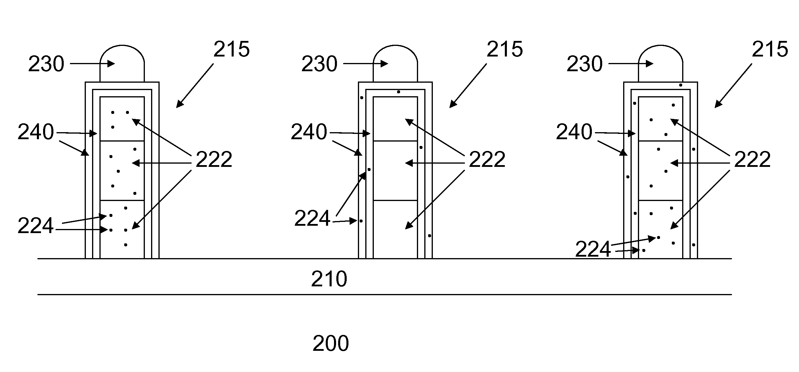
[0040]In this example a comparison is made between the photoluminescence responses of unshelled ZnSe nanowires and shelled ZnSe nanowires, where the shelling material is ZnSeS. Both types of nanowires are formed on Si substrates, where a low energy surface film 210 of silicon oxide is on the surface of the Si. To begin the process the Si substrates are degreased in a sonicator using consecutively acetone, methanol, and water. Next the Si substrates are placed in a conventional dry thermal oxide furnace where 1 micron of oxide is formed on the surface. To form metal alloy nanoparticles 230 of gold-tin the substrates are placed in a conventional thermal evaporator whose base pressure goes down to ˜10−6 torr. Prior to thermal evaporation the substrates are degreased in a sonicator using consecutively acetone, methanol, and water. To form the gold-tin nanoparticles, 1 nm of gold is thermally evaporated, followed by 3 nm of tin.

[0041]Growth of the nanowires occurs in a home-built atmosph...

example 2

[0043]In this example ZnSe / ZnSeS core-shell nanowires are grown where the core ZnSe nanowire is doped with Cl. The growth conditions are analogous to that described in Example 1 for the core-shell nanowires except for the following. The chlorine precursor is butyl chloride. Because small amounts of Cl is required to dope ZnSe highly n-type, the butyl chloride bubbler was cooled to a temperature of −25 C. For the ZnSe:Cl core nanowire growth, 2.8, 15.4 and 0.4 sccm of He—H2 flows through the Zn, Se, and Cl bubblers, respectively, for 65 minutes. Once more there are two ZnSeS shells (35% and 55%). For the 35% ZnSeS shell, 2.8, 10.0, and 9.2 sccm of He—H2 flows through the Zn, Se, and S bubblers, respectively, for 13 minutes. For the 55% ZnSeS shell, 2.8, 6.9, and 14.4 sccm of He—H2 flows through the Zn, Se, and S bubblers, respectively, for 20 minutes.

[0044]FIG. 7 shows representative scanning electron microscope (SEM) images of isolated ZnSe:Cl / ZnSeS core-shell nanowires at two diffe...

example 3

[0045]In the final example multiple quantum wells of ZnSeTe are grown in the core ZnSe nanowires, which once again are shelled with ZnSeS (35% followed by 55%). In order to increase the flow rate of carrier gas through the Zn bubbler, it is cooled to a temperature of −13° C. (enabling a factor of 10 increase in the flow rate). For this example the Au / Sn nanoparticles are formed by thermally evaporating 1.5 nm of Au followed by 4.5 nm of Sn. The Te precursor is diisopropyl telluride. Its bubbler is cooled to −18 ° C. For the ZnSe:ZnSeTe core nanowire growth, 7.7, 7.8 and 30 sccm of He—H2 flows through the Zn, Se, and Te bubblers, respectively. It is to be noted that the Te precursor flow is indicative of approximately an 8% Te concentration in ZnSeTe. The main He—H2 carrier gas flows at 1700 sccm, while the substrate is maintained at 330° C. Starting with the growth of ZnSe for 420 s, the ZnSeTe quantum wells are grown for 5 s, followed by 145 s of a ZnSe barrier section. This sequen...


PUM

PropertyMeasurementUnit
pressureaaaaaaaaaa
pressureaaaaaaaaaa
thicknessaaaaaaaaaa

Abstract

A method of making II-VI core-shell semiconductor nanowires includes providing a support; depositing a layer including metal alloy nanoparticles on the support; and heating the support and growing II-VI core semiconductor nanowires where the metal alloy nanoparticles act as catalysts and selectively cause localized growth of the core nanowires. The method further includes modifying the growth conditions and shelling the core nanowires to form II-VI core-shell semiconductor nanowires.

Description

CROSS-REFERENCE TO RELATED APPLICATION[0001]Reference is made to commonly assigned U.S. patent application Ser. No. ______ filed concurrently herewith, entitled “II-VI Core-Shell Semiconductor Nanowires, by Keith B. Kahen et al, the disclosure of which is incorporated herein.FIELD OF THE INVENTION[0002]The present invention relates to forming low defect II-VI core-shell semiconductor nanowires.BACKGROUND OF THE INVENTION[0003]Worldwide interest in light-emitting diode (LED) technology has rapidly increased over the past two decades. Starting with inorganic LEDs developed in the 60s, they have found their way into numerous lighting, signaling, and display applications, such as, automotive lighting, architectural lighting, flashlights, and backlights for LCD-based displays. Since the turn of the century they have started to appear in more mainstream lighting applications, which as a result of their long life and very high efficacy will result in significant savings in energy usage. Th...

Claims


Application Information

Patent Timeline
Patent Type & Authority Applications(United States)
IPC IPC(8): H01L21/363H01L21/38
CPCB82Y10/00H01L33/18H01L21/02513H01L21/02551H01L21/02557H01L21/0256H01L21/02562H01L21/02568H01L21/02576H01L21/02579H01L21/02603H01L21/02645H01L21/02653H01L29/0665H01L33/0087H01L33/06H01L21/02469
Inventor KAHEN, KEITH B.HOLLAND, MATTHEW
Owner NANOCO TECH LTD
Why Eureka
Try Eureka