Reflective anode and wiring film for organic el display device
- Summary
- Abstract
- Description
- Claims
- Application Information
AI Technical Summary
Benefits of technology
Problems solved by technology
Method used
Image

Examples
example 1
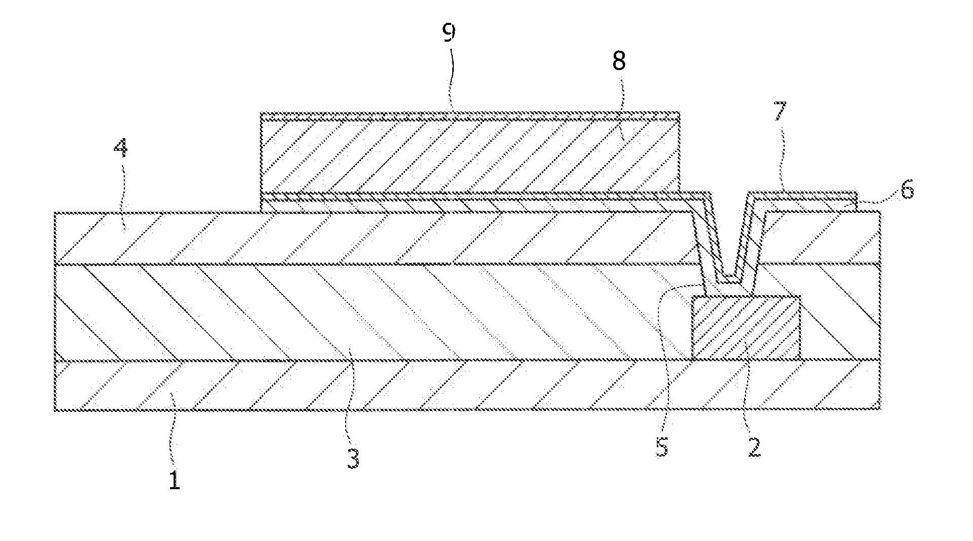
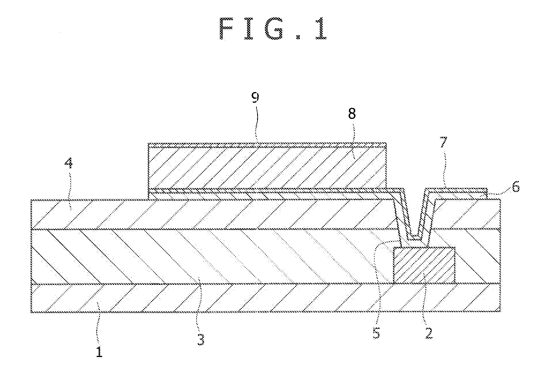
[0068]Using a disk-like glass (Corning non-alkaline glass #1737, diameter: 50 mm, thickness: 0.7 mm) as a material for the substrate 1, a SiN film of the passivation film 3 was deposited at a substrate temperature: 280° C., and with a thickness: 300 nm. Further, using a DC magnetron sputtering device, on the surface of the passivation film 3, there were deposited 1000-angstrom-thick Ag-based alloy film 6 of Ag-(X)Nd-(Y)Cu (X: 0.2 to 0.7 at %, Y: 0.3 to 0.9 at %) and Ag-based alloy film 6 of Ag-(X) Bi (X: 0.1 to 1.0 at %) thin film. The deposition conditions at this step were as follows. Substrate temperature: room temperature, Ar gas pressure: 1 to 3 mTorr, interpole distance: 55 mm, and deposition rate: 7.0 to 8.0 nm / sec. Further, the ultimate vacuum before deposition of the Ag-based alloy film 6 was 1.0×10⁻⁵ Torr or less.
[0069]Then, samples in each of which deposition of the Ag-based alloy film 6 had been completed were divided into three groups (A to C). The samples of Group A we...
example 2
[0079]Using a disk-like glass (Corning non-alkaline glass #1737, diameter: 50 mm, thickness: 0.7 mm) as a material for the substrate 1, a SiN film of the passivation film 3 was deposited at a substrate temperature: 280° C., and with a thickness: 300 nm on the surface of the substrate 1. Further, using a DC magnetron sputtering device, an Ag-based alloy film of Ag-0.1Bi-0.2Nd, and an Ag-based alloy film 6 of Ag-0.1Bi-0.1Ge were deposited with a thickness of 1000 angstrom on the surface of the passivation film 3. The deposition conditions at this step were as follows. Substrate temperature: room temperature, Ar gas pressure: 1 to 3 mTorr, interpole distance: 55 mm, and deposition rate: 7.0 to 8.0 nm / sec. Further, the ultimate vacuum before deposition of the Ag-based alloy film 6 was 1.0×10⁻⁵ Torr or less.
[0080]Then, samples in each of which deposition of the Ag-based alloy film 6 had been completed were subjected to a heat treatment at a heat treatment temperature: 250° C., for a heat...
example 3
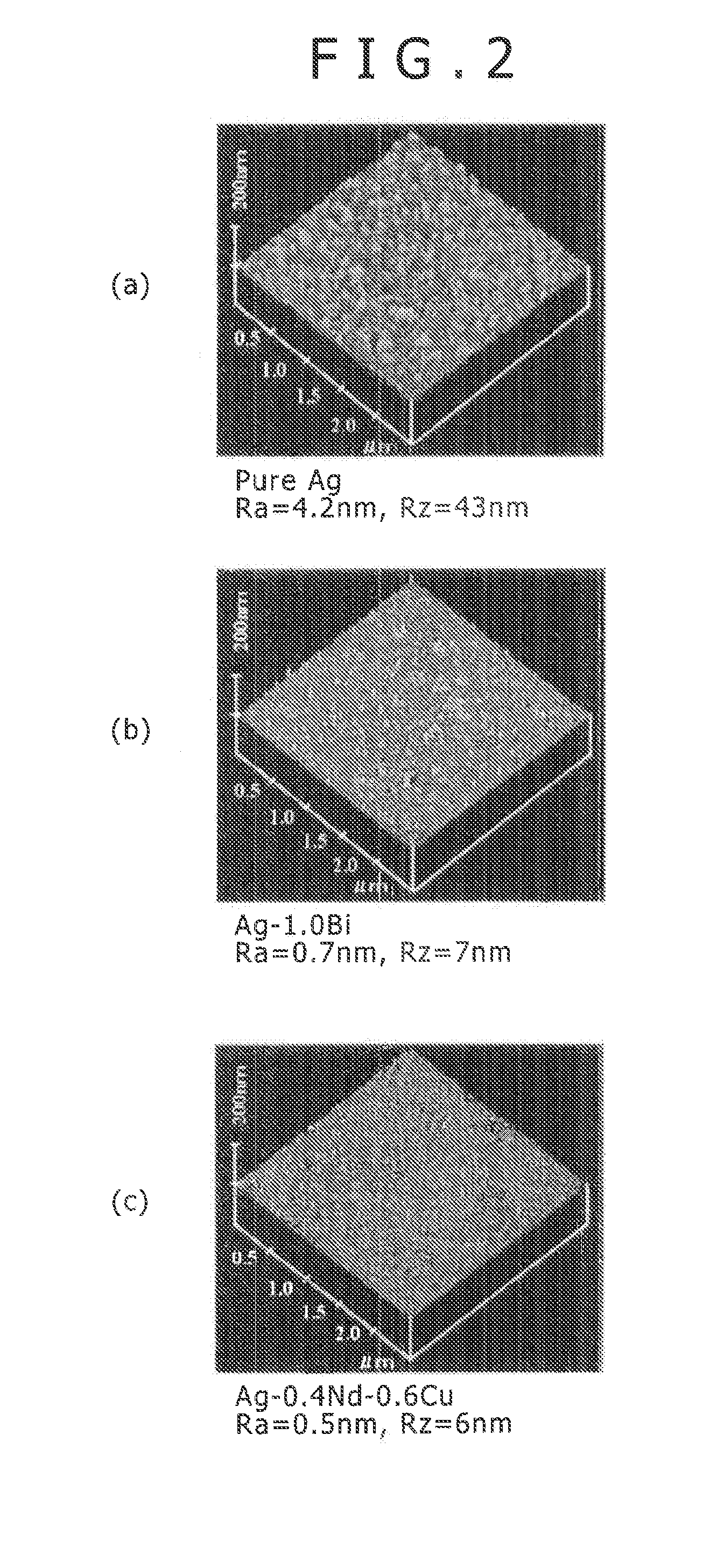
[0084]Out of the samples of the group A of Example 1, the ones in each of which the material for the Ag-based alloy film 6 was Ag-(X)Nd-(Y)Cu alloy (X: 0.7 at %, Y: 0.9 at %) were subjected to an environmental test (Aging Test). The environmental test was performed by exposing each sample under environment of a temperature of 80° C. and a humidity of 90% for 48 hours. Thus, the changes in surface roughness by AFM measurement were observed. FIG. 4 shows the results.
[0085]As apparent from FIG. 4, for the Ag-based alloy films in the present invention, the surface smoothness immediately after deposition (as-depo) is higher than that of pure Ag, and this scarcely changes even after the environmental test. This indicates that the aggregation resistance is improved by addition of Nd and Cu. In the present example, the example of Ag—Nd—Cu alloy was shown. However, even the Ag—Bi alloy provided the same results.
PUM
| Property | Measurement | Unit |
|---|---|---|
| Fraction | aaaaa | aaaaa |
| Percent by atom | aaaaa | aaaaa |
| Mean roughness | aaaaa | aaaaa |
Abstract
Description
Claims
Application Information
 - R&D
- Intellectual Property
- Life Sciences
- Materials
- Tech Scout
- Unparalleled Data Quality
- Higher Quality Content
- 60% Fewer Hallucinations
Browse by: Latest US Patents, China's latest patents, Technical Efficacy Thesaurus, Application Domain, Technology Topic, Popular Technical Reports.
© 2025 PatSnap. All rights reserved.Legal|Privacy policy|Modern Slavery Act Transparency Statement|Sitemap|About US| Contact US: help@patsnap.com