Transparent conductive film and photoelectric converion element

a technology of transparent conductive film and converion element, which is applied in the direction of oxide conductors, conductors, non-metal conductors, etc., can solve the problems of limiting achieve the improvement of incident photon-to-current conversion efficiency, conductivity, and sufficient durability

Inactive Publication Date: 2011-10-06
SONY CORP
View PDF1 Cites 17 Cited by
  • Summary
  • Abstract
  • Description
  • Claims
  • Application Information

AI Technical Summary

Benefits of technology

[0011]The transparent conductive film is formed by a multilayer film constituted of the first conductor layer and the second conductor layer having a higher resistance than the first conductor layer. Since the second conductor layer has a specific resistance of 1*106 Ω*cm or less, an increase of the sheet resistance of the entire film is suppressed and can be made about the same level as the sheet resistance of the first conductor layer alone. Moreover, lowering of transparency is also suppressed. In addition, since a titanium oxide has excellent durability with respect to acid, by covering the first conductor layer with the second conductor layer that includes a titanium oxide, it becomes possible to effectively protect the first conductor layer from acid.
[0012]An increase of a sheet resistance with respect to a sheet resistance of the first conductor layer alone, which is obtained after the second conductor layer is laminated, is 10Ω / □ or less. With this structure, the protective effect of the first conductor layer can be obtained without impairing low resistance characteristics.
[0013]The first transparent conducting oxide may be a tin oxide including indium (ITO). With this structure, the resistance of the first conductor layer can be easily lowered.
[0020]In the photoelectric conversion element, the first electrode has transparency, conductivity, and sufficient durability with respect to an electrolyte with a strong oxidation nature. Therefore, with the conversion element, it is possible to improve the incident photon-to-current conversion efficiency by a low resistance of the negative electrode and prevent the incident photon-to-current conversion efficiency from being lowered with time due to corrosion prevention of the negative electrode.
[0021]The oxide semiconductor layer may be formed of a porous titanium oxide. With this structure, since the oxide semiconductor layer and the second conductor layer are formed of the same type of material, a transportation efficiency of electrons from the oxide semiconductor layer to the first electrode can be enhanced and the incident photon-to-current conversion efficiency can be improved.
[0022]According to the embodiments of the present invention, a transparent conductive film having excellent transparency, conductivity, and corrosion resistance can be obtained. Moreover, a photoelectric conversion element with which an incident photon-to-current conversion efficiency can be improved can be obtained.

Problems solved by technology

However, since the FTO film has a higher resistivity than other transparent conductive oxides such as a zinc oxide (ZnO) and an indium tin oxide (ITO), there has been a limit in improving an incident photon-to-current conversion efficiency.
On the other hand, since ITO films and zinc oxide-based transparent conductive films have poor acid resistance, there has been a problem in applying them to solar cells that use an electrolyte having strong corrosiveness.

Method used


Image

  • Transparent conductive film and photoelectric converion element
  • Transparent conductive film and photoelectric converion element
  • Transparent conductive film and photoelectric converion element

Examples


first embodiment

Photoelectric Conversion Element

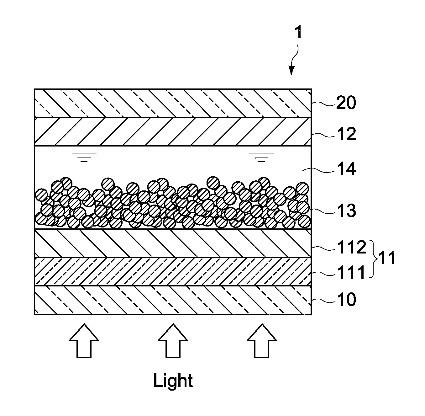
[0029]FIG. 1 is a schematic cross-sectional diagram of a photoelectric conversion element according to a first embodiment of the present invention. Hereinafter, a photoelectric conversion element 1 of this embodiment will be described.

[0030]The photoelectric conversion element 1 of this embodiment is constituted of a dye-sensitized solar cell. The photoelectric conversion element 1 includes a negative electrode 11 as a collective electrode, a positive electrode 12 as an antipole, an oxide semiconductor layer 13, and an electrolyte layer 14. The negative electrode 11 and the positive electrode 12 are connected to a negative electrode and a positive electrode of an external circuit (load) (not shown). The oxide semiconductor layer 13 is in contact with the negative electrode 11 and formed of a porous titanium oxide. The oxide semiconductor layer 13 supports a pigment whose electrons are excited by visible light irradiated onto the pigment, for example. ...

second embodiment

[0054]FIG. 3 is a schematic cross-sectional diagram of a photoelectric conversion element according to a second embodiment of the present invention. Portions that correspond to those of the first embodiment above in the figure are denoted by the same reference numerals, and detailed descriptions thereof will be omitted.

[0055]In a photoelectric conversion element 2 of this embodiment, a negative electrode 21 differs from that of the first embodiment and includes a multilayer structure constituted of the first conductor layer 111, the second conductor layer 112, and a third conductor layer 113. The third conductor layer 113 is provided inside the first conductor layer 111 and has a specific resistance (third specific resistance) smaller than that of the first conductor layer 111. Specifically, the third conductor layer 113 is constituted of a metal wiring of silver (Ag), an alloy thereof, and the like, though the metal type is not limited thereto. Alternatively, conductive materials o...


PUM

PropertyMeasurementUnit
specific resistanceaaaaaaaaaa
thicknessaaaaaaaaaa
thicknessaaaaaaaaaa

Abstract

A transparent conductive film includes: a first conductor layer formed of a first transparent conducting oxide having a first specific resistance; and a second conductor layer that is laminated on the first conductor layer, has a second specific resistance that is equal to or larger than the first specific resistance and equal to or smaller than 1*106 Ω*cm, and is formed of a second transparent conducting oxide including titanium.

Description

BACKGROUND OF THE INVENTION[0001]1. Field of the Invention[0002]The present invention relates to a transparent conductive film having corrosion resistance and a photoelectric conversion element including the transparent conductive film.[0003]2. Description of the Related Art[0004]In recent years, dye-sensitized solar cells as one of photoelectric conversion elements are being developed. A dye-sensitized solar cell includes a semiconductor layer that supports a pigment, a negative electrode that comes into contact with the semiconductor layer, an electrolyte, and a positive electrode opposing the semiconductor layer with the electrolyte interposed between the positive electrode and the electrolyte. The pigment emits electrons by light entering the semiconductor layer, and the emitted electrons are transported to the negative electrode via the semiconductor layer. The negative electrode and the positive electrode are connected to an external circuit, and the electrons that have reache...

Claims


Application Information

Patent Timeline
Patent Type & Authority Applications(United States)
IPC IPC(8): H01L29/12H01B5/00
CPCH01G9/2031B32B15/085B32B15/02B32B2457/12H01G9/2068B32B2457/00C23C14/083Y02E10/542B32B15/09C23C14/086H01B1/08H01L51/442B32B15/08B32B2307/202B32B15/043H01G9/2059B32B27/36B32B27/365B32B2307/412B32B2307/714B32B2457/202B32B2457/206B32B2457/208H10K30/82
Inventor SEKINE, MASAAKISAKURAI, KYOKOONODERA, SEIICHI
Owner SONY CORP
Why Eureka
Try Eureka